Lab 4 - EE 421L
Authored
by Adrian Angelo G Fuerte,
Rebelmail: fuerta1@unlv.nevada.edu
09/25/2019
Pre-Lab
The pre-lab consisted of reading through Lab 4 itself and going through Tutorial 2 which
instructs us to make both the layouts and schematics of PMOS and NMOS.
We then simulated both circuits and got their IV curves. For this
pre-lab I began by creating a new library and copied Tutorial 1 to that
new folder (make sure to chek the box that says update instances under
options). Below are images from Tutorial 2.
New Library Created

Images from Tutorial 2


Lab
description
For
Laboratory 4, we are tasked to generate a total of 4 schematics and
simulations which includes a layout for both the NMOS and PMOS devices.
We will also be creating a probe pad layout which will be connected to
the four terminals (Source, Drain, Gate, and Body) of our NMOS and PMOS
devices.
NMOS (ID v VDS)
For this part of our lab, we are
going to be creating a schematic of an NMOS device for simulating ID v.
VDS for VGS varying from 0V to 5V in 1V steps while VDS varies from 0V
to 5V in 1 mV steps using a 6u/600n width-to-length ratio. I also created a symbol for the NMOS as seen in the images below.
To start off, I navigated to the component browser (bindkey I) -->
select NCSU_Analog_Parts library --> N_Transistors -->nmos4.
NMOS Schematic
NMOS Symbol
NMOS Simulation Schematic

After
creating the simulation schematic for NMOS, I started setting up the
simulation by first selecting the NMOS model file (ami06N.m) from the
ncsu-cdk-1.6.0.beta libary. The following simulation will be a DC
analyses that sweeps VDS from 0 to 5V with 1mV increment. I also used
parametric analysis to sweep VGS along with VDS and the output that
will be plotted is seen in the image below which represents the current
through the drain (Id)
Editing Design Variable

ID v VDS setup

Parametric Analysis (Tool --> Parametric Analysis)
-After setting up the parametric analysis as seen below, press the green button and it will start the simulation and show the plot below.

Plot

NMOS (ID v VGS)
The
next schematic is the same schematic as the first NMOS except we are
simulating ID v VGS. For this schematic, VDS is going to be at a fixed
voltage value of 100mV and VGS will be swept using dc analysis only
(not parametric analysis) from 0V to 2 V with 1 mV increment. We are
going to be using the same model file (ami06N.m). The simulation result
shows that the VGS does not start increasing until the threshold
voltage of 0.7V is reached (shown in the plot below).
DC analysis with VDS at 100mV

Simulation Schematic with VDS at 100mV

Plot

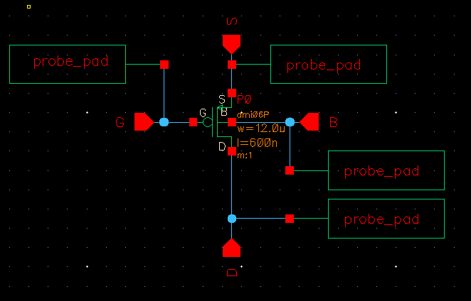
PMOS (ID v VSD)
For
this next step, I created a schematic for my PMOS (the same steps as
creating an NMOS transistor). For this step, VSG is going to vary from
0V to 5V in 1 V steps while VSD varies from 0V to 5V in 1mV steps. I
will be using a 12u/600n width-to-length ratio for the PMOS device. The
model file that will be used in this simuation is ami06P.m which is
located in the same folder that ami06N.m, it is important to select
ami06P.m or else the simulation will not work.
PMOS Schematic

PMOS Model

PMOS Symbol

PMOS Simulation Schematic

Plot Result

PMOS (ID v VSG)
The
second schematic for the PMOS is the same schematic as the last one but
VSD will be at a fixed voltage of 100mV and swept from 0V to 2V with
1mV increment. The same model file will be used and only DC analysis
will be required to use not parametric analysis. The resulting plot
will look the same as the plot from NMOS ID vs VGS but the threshold
for the PMOS is a little higher at about 0.9V compared to the NMOS's
0.7V threshold.
Simulation Schematic
 Plot
Plot

The
next step after the simulations for NMOS and PMOS is to create a layout
for both devices and connect all four terminals to probepads. For the
first layout, an NMOS device will be used with a size of 6u/0.6u
width-to-length ratio. Before starting to make the layout I first
copied the cells to make the probe pad to be instantiated later onto my
NMOS and PMOS devices from Lab4.
Probe Pad Schematic

Probe Pad Symbol

Probe Pad Layout

NMOS Layout
After
copying the files onto my Lab folder, I started by instantiating my
NMOS layout and sizing it to 6u/0.6u. This layout can be found in the
NCSU_Techlib_ami_06 library when instantiating with the bindkey I.
NMOS Layout (without connections to probes. NOTE: gnd! is B)

NMOS schematic with pads

NMOS Layout with probe connections to S, G, D, B


DRC and LVS verification


PMOS Layout
The
last step in this lab is to create a layout for the PMOS that will have
a size of 12u/0.6u. This PMOS transistor is also found in the
NCSU_Techlib_ami06 library.
PMOS Layout (without probes)

PMOS Schematic
PMOS Layout with probes

DRC and LVS verification for PMOS


Return to EE421L Students
Return to My Lab Directory