 ->
-> 
Lab Project - EE 421L - Fall 2019
Design a Circuit that takes a 9-11MHz Clock Signal and Generates a 36-44MHz Clock Signal (x4 Clock Multiplier)
Rebelmail: buenj1@unlv.nevada.edu
Project Description:
Design
a circuit that takes a 9-11 MHz clock signal and generates a 36-44 MHz
clock signal. In other words, design x4 clock multiplier. The input
clock is multiplied by 4 and output. Assume the input clock signal has
a 50% duty cycle.
->
In this project, the XOR gate is used as an edge detector
for the input signal when applied a delayed signal from one input (A)
onto the other input (B). Thereby, the resulting output signal of
 ->
-> 

->
Simulation Schematic for the 2 buffers and Symbol
First Delay Buffer (1st XOR gate) Symbol
 ->
->
| The combined buffers are put together into one, leading
to 1 overall symbol for the two buffers (shown above) The two buffers are combined together to make a total of 6 inverters. The delay is implemented in the delay buffer and getting fast edges on the signal is implemented on the "Fast" buffer. |
First Delay Buffer Simulation (Input signal vs. Delayed Input signal)

| Period = 100ns, pulse width = 50ns (to test for the 10MHz frequency) For the simulation above, I calculated the propagation delays (tPHL and tPLH) Using the widths and lengths used for the delay buffer schematic, W = 12u (PMOS), W = 6u (NMOS), L = 12u (BOTH) | Effective Resistances: PMOS -> Rp = Rp'(L/W) = (40k)(12u/12u) = 40k NMOS -> Rn = Rn'(L/W) = (20k)(12u/6u) = 40k Rp + Rn = 80k Capacitances: PMOS -> Coxp = Cox'(W)(L) = 2.5fF(12u)(12u) = 360fF NMOS -> Coxn = Cox'(W)(L) = 2.5fF(6u)(12u) = 180fF Ctot = 5/2(360fF + 180fF) = 1350fF |
| Taking the sum of both the propagation high to low and low to high delays and dividing that number by the number of inverters used for the 'delay' buffer (N = 3) gave me an approximate delay of 25.2 ns as shown in the simulation above. | tPHL + tPLH = 0.7(Rp + Rn)(Ctot) = 0.7(80k)(1350fF) = 75.6ns (tPHL + tPLH) / 3 = 25.2ns |
Simulation of the 2x CLK


The 2x CLK output shown above had slow edges, which can have an influence in it's delayed signal and the 4x CLK signal.
-->TO FIX: Include a buffer at the output of the first XOR gate
2x CLK Output Buffer (12u/6u, L = 600n, m = 2) Updated Schematic
 ->
->
Resulting simulation:
 **Notice the edges got sharper after including the buffer at the output.
PART 2: MAKING THE 4X CLOCK
Intro: To make the 4x clock, another XOR gate has to be placed in-series with the 1st XOR gate with the input of the 2nd XOR gate be the output of the 1st XOR (2x clk) and it's delayed signal.
Buffer 2 (2nd Delay Buffer on the 2nd XOR Gate):
- This buffer is also composed of a delay buffer and a fast buffer and are then combined together to make one overall buffer for the delayed signal.
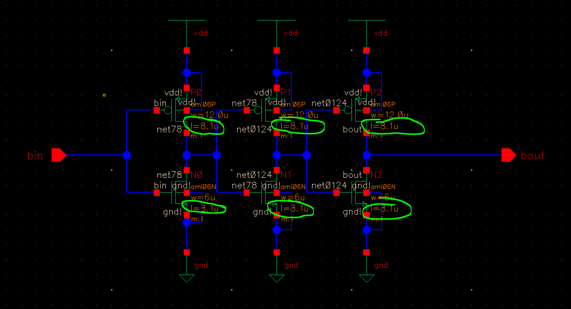
Delay Buffer (12u/6u, L = 8.1u) "Fast" Buffer (12u/6u, L = 600n (minimum))
 ->
->
The 'fast' buffer used here is the exact same schematic used in the previous. The lengths of the 'delay' buffer is smaller than the lengths of the first delay buffer (length ~8u). This is because the delay time for the delayed signal is smaller/quicker than the previous. In order to achieve a near 50% duty cycle for the output, the delay time has to be around 12ns for a 10MHzinput clock. |
Simulation Schematic for the 2 buffers and Symbol
Second Delay Buffer (2nd XOR gate) Symbol
 ->
-> 
Second Delay Buffer Simulation (2x CLK vs. Delayed 2x CLK)

| Period = 50ns, Pulse width = 25ns (to model the 2x CLK Signal) Calculations for the propagation delays Using widths and lengths according to the delay buffer schematic: W = 12u (PMOS), W = 6u (NMOS), L = 8.1u (BOTH) | Effective Resistances: PMOS -> Rp = Rp'(L/W) = (40k)(8.1u/12u) = 27k NMOS -> Rn = Rn'(L/W) = (20k)(8.1u/6u) = 27k Rp + Rn = 54k Capacitances: PMOS -> Coxp = Cox'(W)(L) = 2.5fF(12u)(8.1u) = 243fF NMOS -> Coxn = Cox'(W)(L) = 2.5fF(6u)(8.1u) = 121.5fF Ctot = 5/2(243fF + 121.5fF) = 911.25fF |
| Taking the sum of both the propagation high to low and low to high delays and dividing that number by the number of inverters used for the 'delay' buffer (N = 3) gave me an approximate delay of 11.5 ns as shown in the simulation above | tPHL + tPLH = 0.7(Rp + Rn)(Ctot) = 0.7(54k)(911.25fF) = 34.4ns (tPHL + tPLH) / 3 = 11.5ns |
Simulating the 4x CLK
Schematic

Simulation of the 4x CLK

| For the simulation above, the 4x output is slightly slow in terms of it's rise times. To sharpen the rise times, a buffer would have to be included at the output of the 4x clock |
4x CLK Output Buffer (12u/6u, L = 600n, m = 2, using 2 inverters)

Updated Circuit and Resulting Simulation
Schematic

Simulation with included buffer at the output

| **Note: The pins in the middle of the circuit are there so I can see the signals operating at those nodes when I simulate the circuit. They will be removed in the final schematic. |
Temporary Sim-Schematic to Simulate ALL Signals

| The sim-schematic above is created based on the previous 4x schematic that included each of the pins for all signals. The schematic is used to simulate all signals from the input signal (10MHz) to the 2x CLK and to the 4x CLK as well as their corresponding delayed signals. |
Simulation of ALL Signals (with the input clock at 10MHz, 100ns period, and with VDD = 5V)

| The resulting frequency of the 4x Clock signal with a 10MHz input signal is calculated to be around 41MHz. |
Final Schematic and Symbol
Schematic (INPUT - "clk_in", OUTPUT - "clk_out")

Symbol

PART 3: Test for Other Frequencies and Power Supply Voltages (VDD)
Frequency - 9MHz
| 9MHz, VDD = 4V |  |  |
| 9MHz, VDD = 5V |  |  |
| 9MHz, VDD = 6V |  |  |
| 9MHz, VDD = 7V |  |  |
Frequency = 10MHz
| 10 MHz, VDD = 4V |  |  |
| 10 MHz, VDD = 5V |  |  |
| 10 MHz, VDD = 6V |  |  |
| 10 MHz, VDD = 7V |  |  |
Frequency = 11 MHz
| 11 MHz, VDD = 4V |  |  |
| 11 MHz, VDD = 5V |  |  |
| 11 MHz, VDD = 6V |  |  |
| 11 MHz, VDD = 7V |  |  |
PART 4: LAYOUT OF 4X CLOCK MULTIPLIER
Layout and Extracted View of the XOR Gate


DRC and LVS of XOR Gate:


Layout and Extracted View of the 'Delay Buffers'
Delay Buffer 1: Widths - 12u/6u, Lengths (both PMOS and NMOS) - 12u Delay Buffer 2: Widths - 12u/6u, Lengths(both) - 8.1u


Extracted Views
Delay Buffer 1 (length = 12u) Delay Buffer 2 (length = 8.1u)


DRC/LVS of Delay Buffer 1 (length = 12u)
 ->
-> 
DRC/LVS of Delay Buffer 2 (length = 8.1u)
 ->
-> 
Layout and Extracted View of the 'Fast' Buffer (for having fast edges on the signals)
12u/6u, Length = 600n (minimum)
 ->
-> 
DRC/LVS of the 'Fast' Buffer
 ->
-> 
Layout and Extracted View of the First Delay Buffer

| The first delay buffer layout is composed of the delay buffer with the length of 12u and the 'fast' buffer with minimum length of 600n. Both have PMOS and NMOS width sizes of 12u/6u respectively. |
Extracted View

DRC/LVS of the First Delay Buffer
 ->
-> 
Layout of the Second Delay Buffer

| The Second Delay Buffer is composed of the delay buffer with length of 8.1u and the fast buffer with minimum length of 600n. Both have NMOS and PMOS width sizes of 12u/6u respectively. |
Extracted View

DRC/LVS of the Second Delay Buffer
 ->
-> 
Layout and Extracted View of the 2x Clock and the 4x Clock Output Buffers
2x Clock Output Buffer 4x Clock Output Buffer


| 2x Clock Output Buffer: width - 12u/6u, length - 600n (minimum), factor of 2 for each inverter size, 4 inverters used | 4x Clock Output Buffer: width -> 12u/6u, length -> 600n (minimum), factor of 2 for each inverter size, 2 inverters used |
Extracted View
2x Clock Output Buffer 4x Clock Output Buffer


DRC/LVS of the 2x Clock Output Buffer
 ->
-> 
| The LVS output shown in both the 2x or 4x output buffers have more instances for the layout than the schematic. That is due to the increasing multiplier value for the sizes of each inverter of both buffers. |
DRC/LVS of the 4x Clock Output Buffer
 ->
-> 
Entire Layout of the 4x Clock Multiplier Circuit

Extracted View

DRC and LVS Verification
 ->
->  ->
-> 
That concludes my Lab Project.