 ->
->  ->
->  ->
-> 
Lab 4 - EE 421L - Fall 2019
IV Characteristics and Layout of NMOS and PMOS Devices in ON's C5 Process
Rebelmail: buenj1@unlv.nevada.edu
-> -> ->
Lab 4 consists of making 4 schematics, 2 layouts, and simulations involving NMOS and PMOS transistors. In addition, there must also be a probe pad layout that will later be instantiated and connected
to the four terminals of the MOSFETs (Source, Drain, Gate, and Body).
First NMOS (ID v. VDS)
Once logged into Cadence, I began with an NMOS schematic with dimensions of 6u/600n (width/length). The simulation of this transistor will be ID v. VDS, where VDS will be swept from 0 to 5V with 1mV increments along with a varying VGS from 0 to 5V with 1V increments. To use an NMOS transistor, navigate through Component Browser (bindkey I), select the NCSU_Analog_Parts library, choose N_Transistors, and select 'nmos4'.
Setup of the dimensions of the NMOS shown below.


Below is the schematic and symbol view for the 6u/600n NMOS transistor.
Schematic Symbol
 ->
-> 
As shown above, the body of the NMOS transistor is connected to ground (gnd!).
Prior to simulation, a 'sim' schematic must be created in order to simulate the schematic. To sweep VDS and VGS, a voltage source connected to ground must be placed on the gate of the MOSFET for VGS and
another source placed at the drain of the MOSFET for VDS.

The image above is identical to the schematic made during Tutorial 2 except with the V1 instance renamed to VDS.
To setup the simulation, the NMOS model file (ami06N.m) must be selected and included from the 'ncsu-cdk-1.6.0.beta' library. The type of analysis will be a DC analysis, sweeping VDS from 0 to 5V with 1mV increments.
I also added the VGS variable (on ADE L window: Variable -> Edit) which will then be used for parametric analysis (Tool -> Parametric Analysis) so that I will be able to sweep VGS along with VDS. The output plotted
will be the current through the drain of the MOSFET (ID).
 ->
->  ->
-> 
-> 
Once the green button is pressed (on the Parametric Analysis window), the simulation begins to run. The result of the simulation is shown below.
The graph above shows an IV curve of the NMOS relating VDS (sweep), VGS (varying at different voltages/steps), and ID (current at drain).
Second NMOS (ID v. VGS)
The next schematic to do is a second NMOS transistor but by simulating ID v. VGS. For this schematic, VDS will be at a fixed voltage of 100mV and VGS will be swept from 0 to 2V with 1mV increments. The steps of making
this schematic and doing its simulation is almost the same as the previous NMOS, but with small changes.
- same model file is used (ami06N.m)
- same schematic, but VDS is at a fixed voltage
- VGS is swept
- only DC analysis is used, no parametric analysis
Sim schematic of NMOS with VDS @ 100mV

DC analysis for VGS
Simulation result (ID v. VGS)
 ->
-> 
Based on the simulation, at a fixed VDS voltage of 100mV, VGS doesn't start increasing until up to a certain voltage (threshold voltage ~0.65V).
The next step is to make the PMOS transistors and its simulations. The first PMOS involves the ID v. VSD curve and the second involves the ID v. VSG curve with VSD at 100mV.
Similar steps from the first two NMOS transistors but with small changes.
 ->
-> 
 ->
-> 

Sim Schematic DC analysis
 ->
-> 
Simulation result

Almost identical to the ID v. VGS curve (threshold voltage is a little higher)
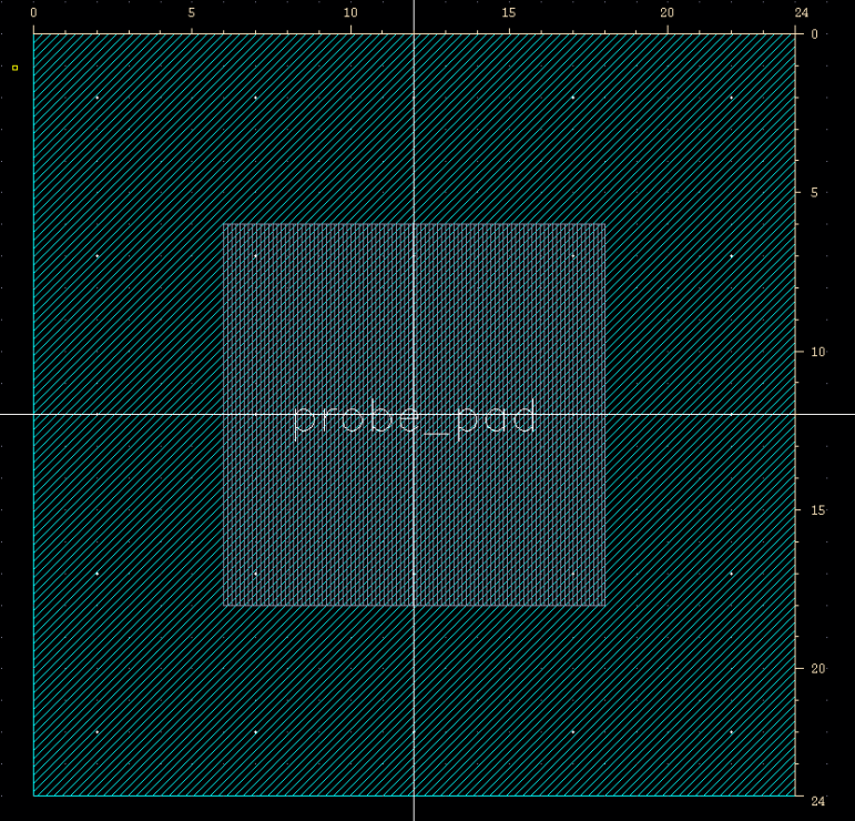
Before the layouts of an NMOS and PMOS transistor, a probe pad must be layed out first (to instantiate later). Going through Tutorial 6, I made a probe pad that is smaller in size (24u by 24u) so that it will be
easier to see the layout involving the MOSFETs and it's connections to the probe pads.
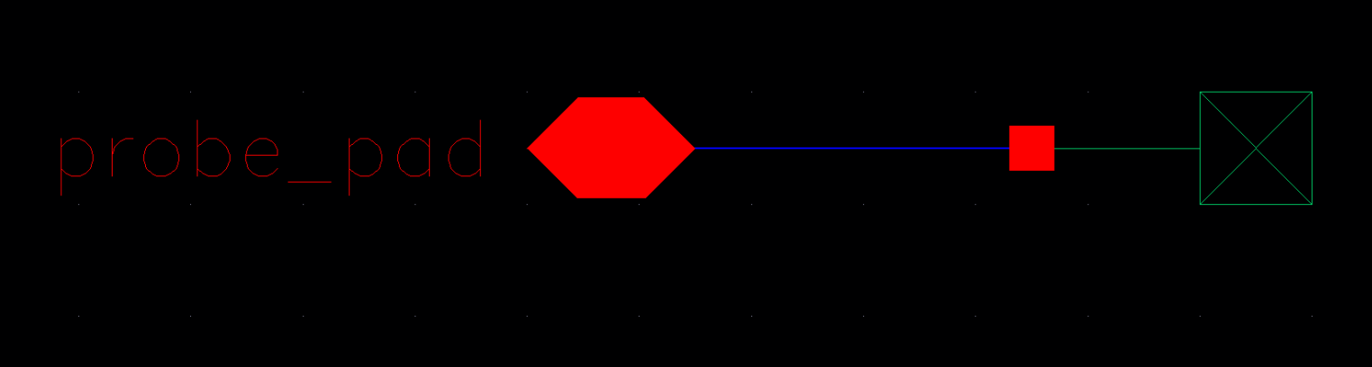
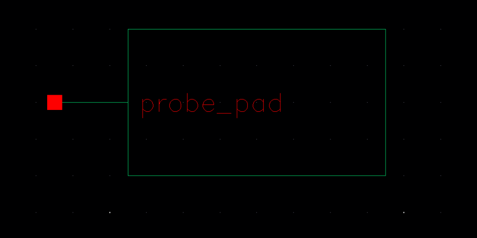
Probe pad schematic and symbol
 ->
-> 
Probe pad layout
 ->
->
The probe pad is only consisting of the metal3 layer and the glass layer. According to the submicron rules, the glass layer has to have edges that are at least 6 microns away from the edges of the metal3 layer.
After the making of the probe pad, I can then use it to instantiate for the NMOS and PMOS layouts. The NMOS and PMOS layouts will have all 4 of their terminals connected to a probe pad.
NMOS layout
The following NMOS layout will have a size of 6u/0.6u (or 600n).
Layout of NMOS (no connections yet)
 The NMOS transistor can be found in the
NCSU_Techlib_ami06 library when instantiating (bindkey I) and object.
The NMOS transistor can be found in the
NCSU_Techlib_ami06 library when instantiating (bindkey I) and object.
With the following connections made to the probe pads from the 4 terminals of the transistor, the full view of the layout is shown below.
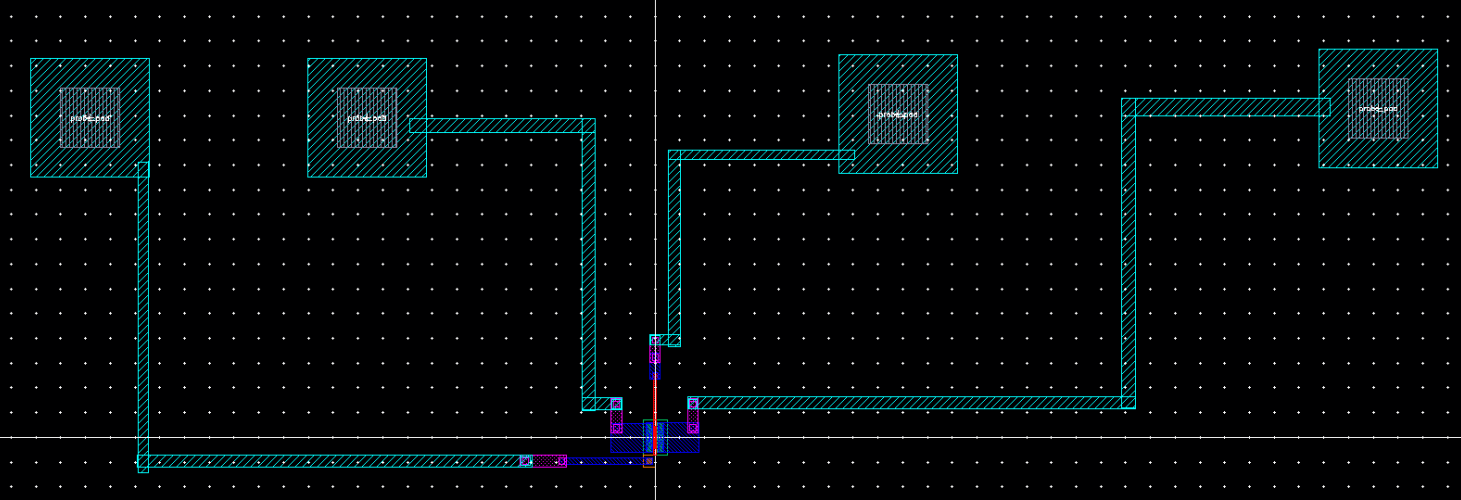
Zoomed in closer to the NMOS..

Note: vias (m3_m2 & m2_m1) are used to connect the metals (metal1, metal2, and metal3 are in different layers, vias must be used to connect them)
Also note: the m1_poly is used to connect the poly layer (in red) to metal1 in order to connect the Gate terminal to a probe pad.
Here is its corresponding schematic view
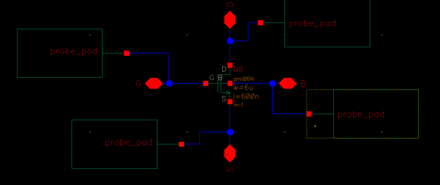
The schematic is made in order to perform LVS.
DRC and LVS verification of the layout.
 ->
-> 
PMOS layout
The following PMOS layout will have a size of 12u/0.6u (or 600n).
Layout of PMOS (with no connections)
 The PMOS transistor is also found in the NCSU_Techlib_ami06 library
With the following connections made to the probe pads from the 4 terminals of the transistor, the full view of the layout is shown below.

Zoomed in closer to the PMOS..

Corresponding schematic view for the PMOS layout
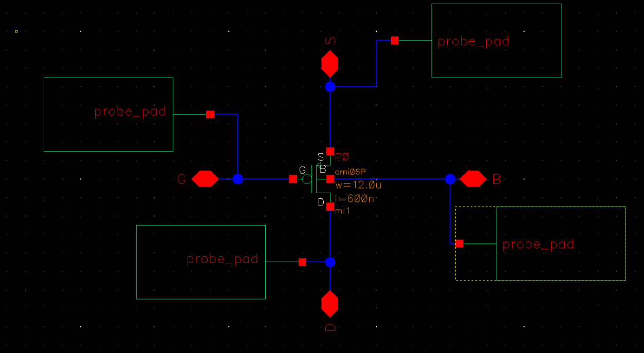
DRC and LVS verification of the PMOS
 ->
-> 