Finish Tutorial 5.
This ends the content of the Prelab.
Create and simulate a 4-wide parallel inverter array.
Comment on the effect of the load capacitors.
Create scheamtics and symbols for NAND, NOR, AND, and OR gates.
Run these gates in parallel (8-wide) to create new 8-bit gates.
Create simulations to demonstrate the operation of these gates.
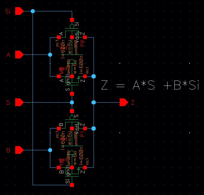
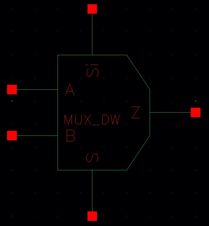
Create the schematic and symbol for a 2-1 MUX/DEMUX.
Show how the circuit can be used for both multiplexing and demultiplexing.
Include an inverter so that only the S input is needed (Si is the compliment of S, henc the inverter).
Create a simulation to show the operation of the 8-bit MUX/DEMUX.
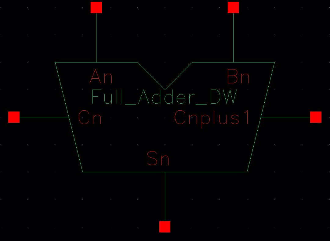
Create a scheamtic and symbol for a Full Adder according to Fig. 12.20 (using 6u/0.6u devices).
Run these Full Adders in series (8-long) to create an 8-bit Full Adder.
Layout both the single Full Adder and the 8-bit Full Adder.
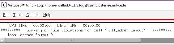
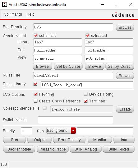
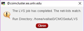
Ensure that the layouts LVS and DRC properly.
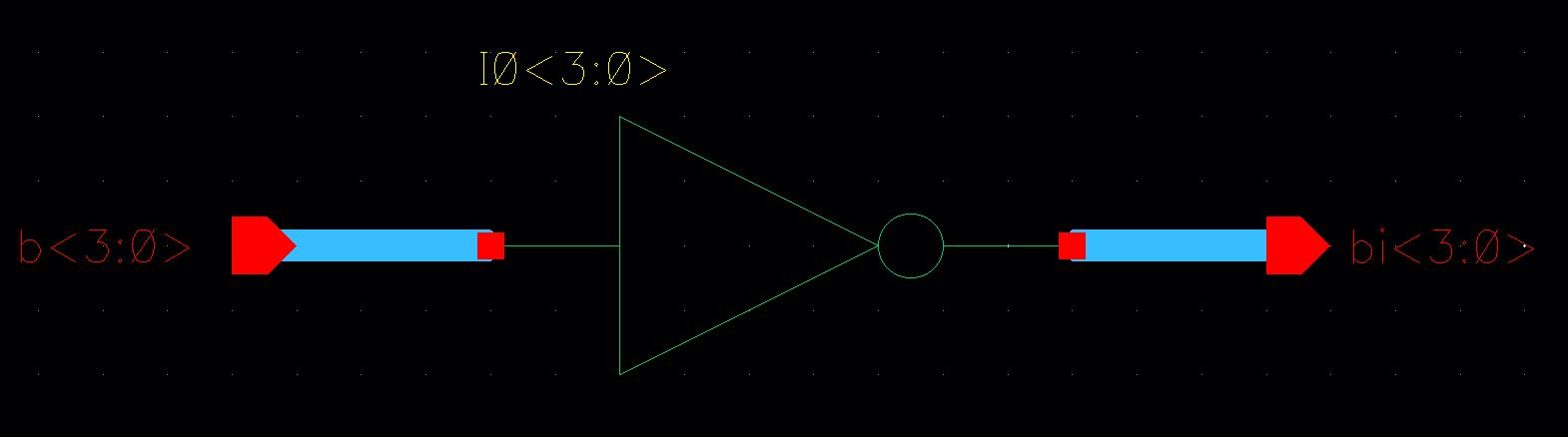
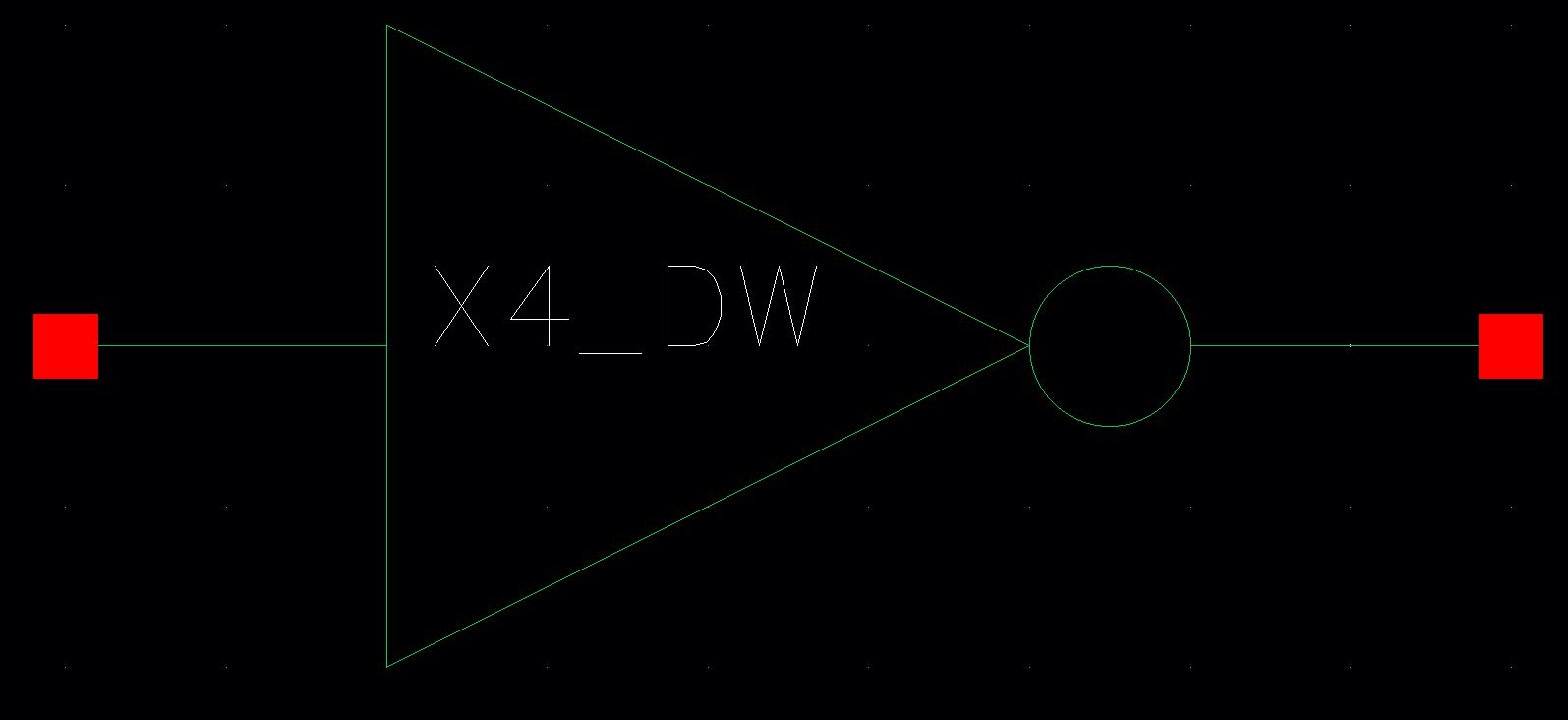
The schematic and symbol for the 4-bit parallel inverter can be seen below:
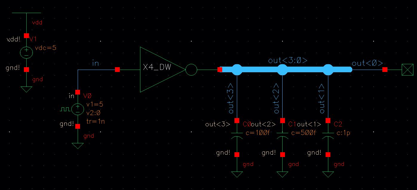
The simulation schematic for analyzing the operation of this 4-bit inverter is shown below:
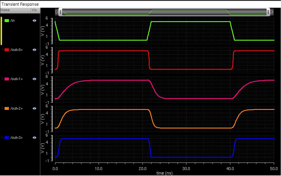
Results from this simulation can be seen below:
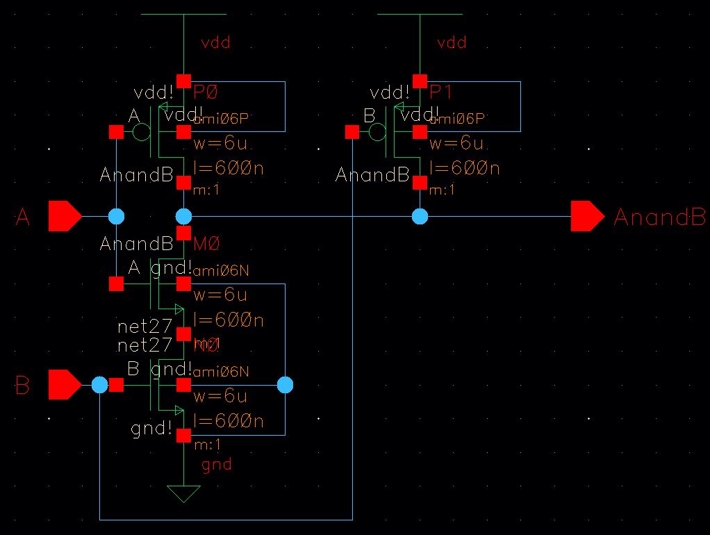
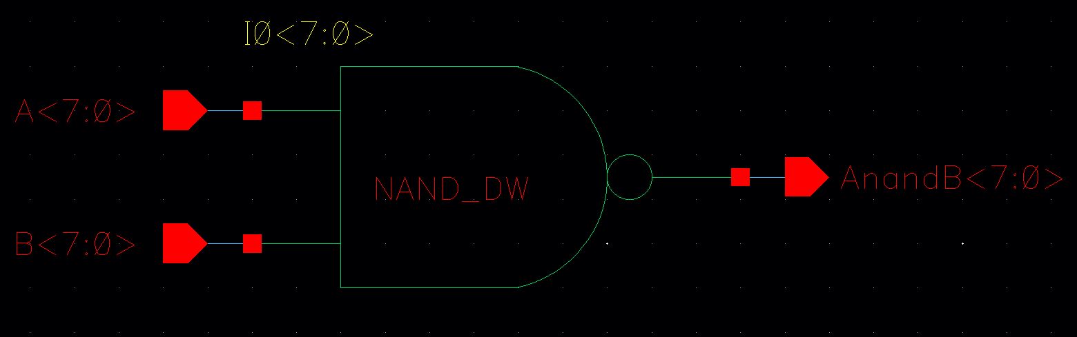
Below shows the schematic and symbol of the 1-bit NAND gate:
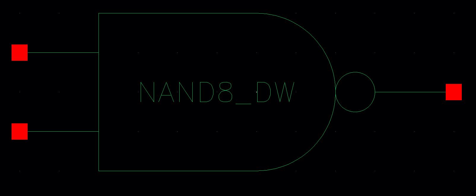
The schematic and symbol for the 8-bit NAND gate can be seen below:
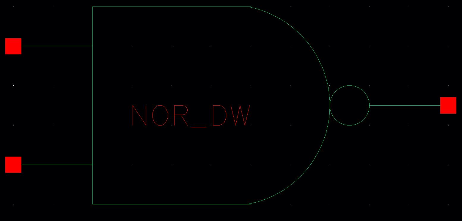
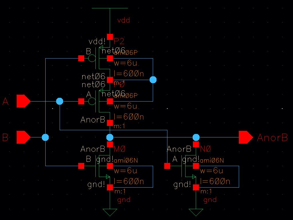
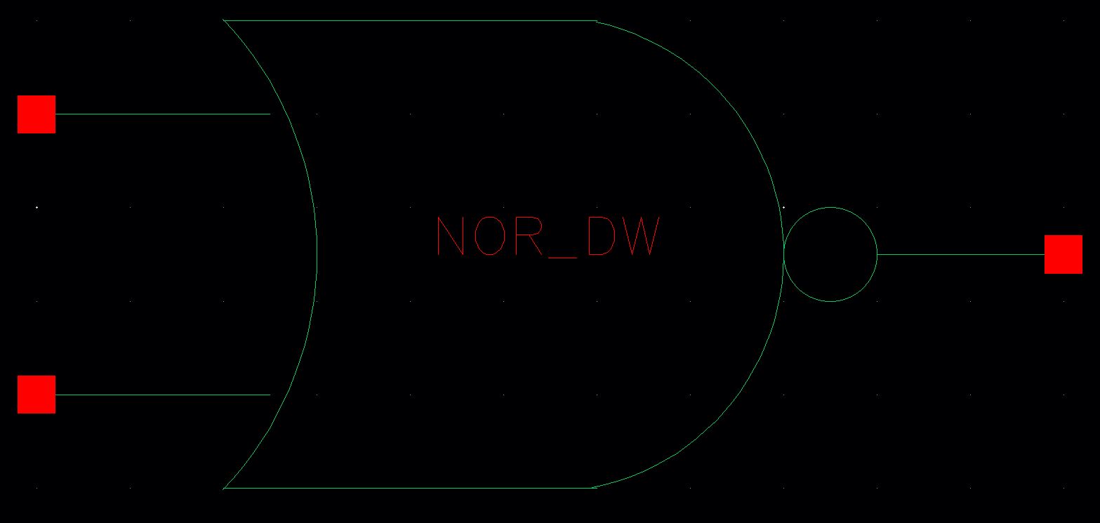
The schematic and symbol for the 1-bit NOR gate can be seen below:
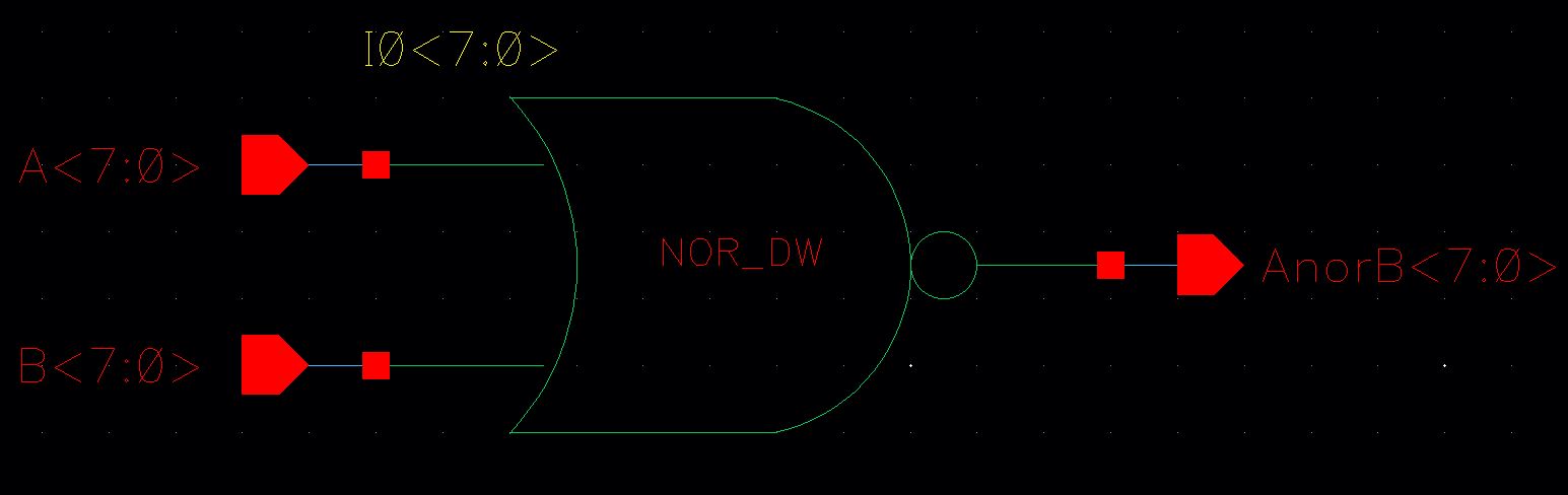
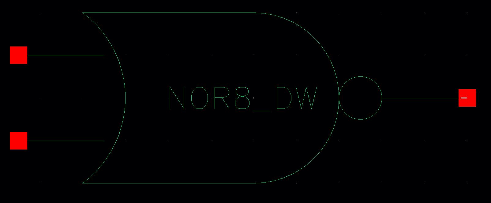
The 8-bit schematic and symbol for the NOR gate can be seen below:
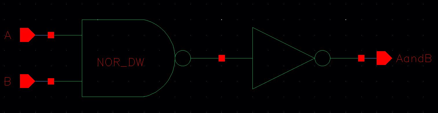
The schametic and symbol for the 1-bit AND gate can be seen below:
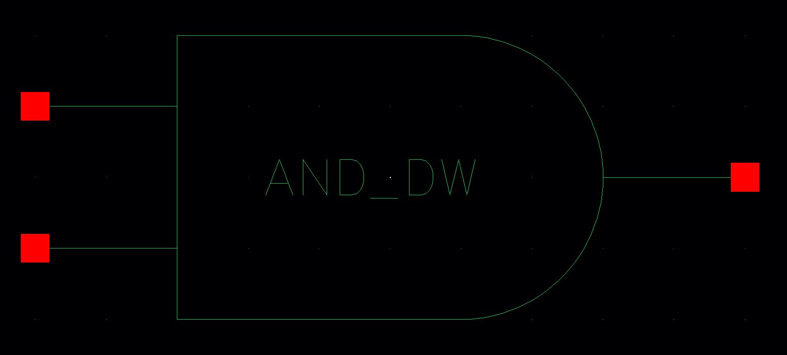
The 8-bit schematic and symbol for the AND gate can be seen below:
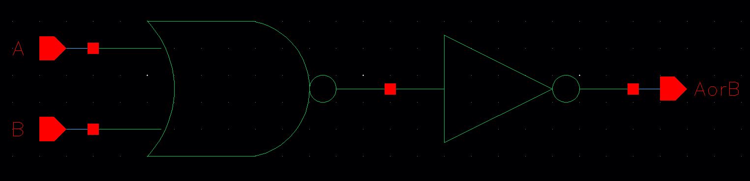
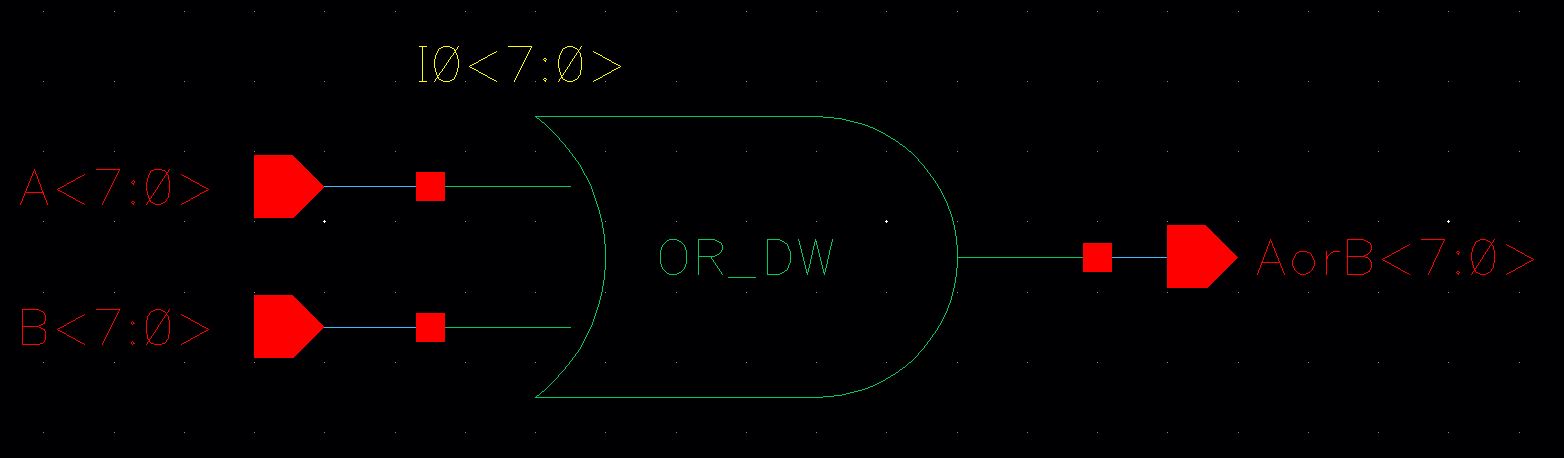
The schematic and symbol for the 1-bit OR gate can be seen below;
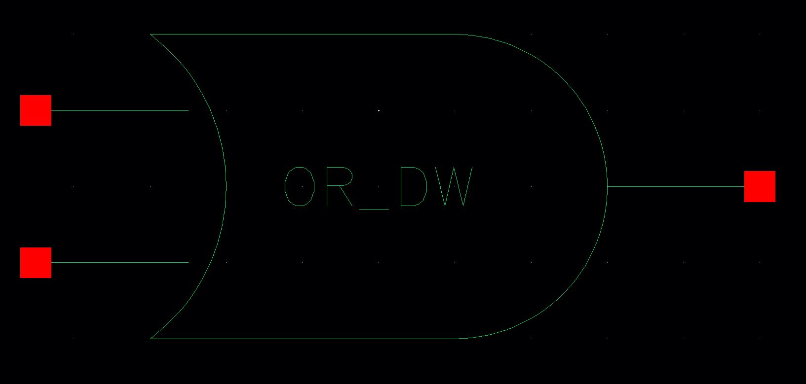
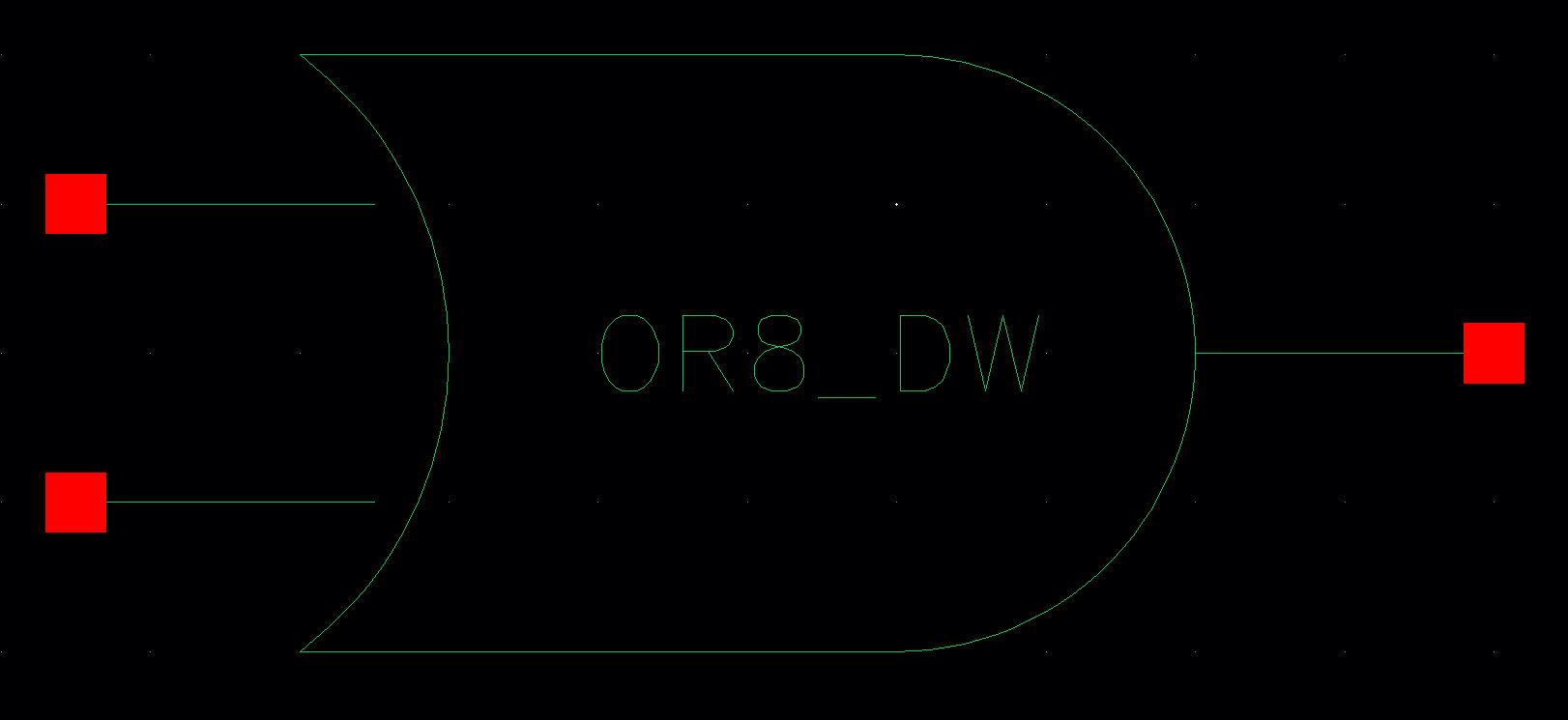
The 8-bit schematic and symbol for the OR gate can be seen below:
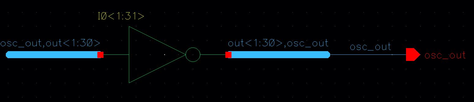
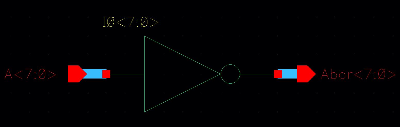
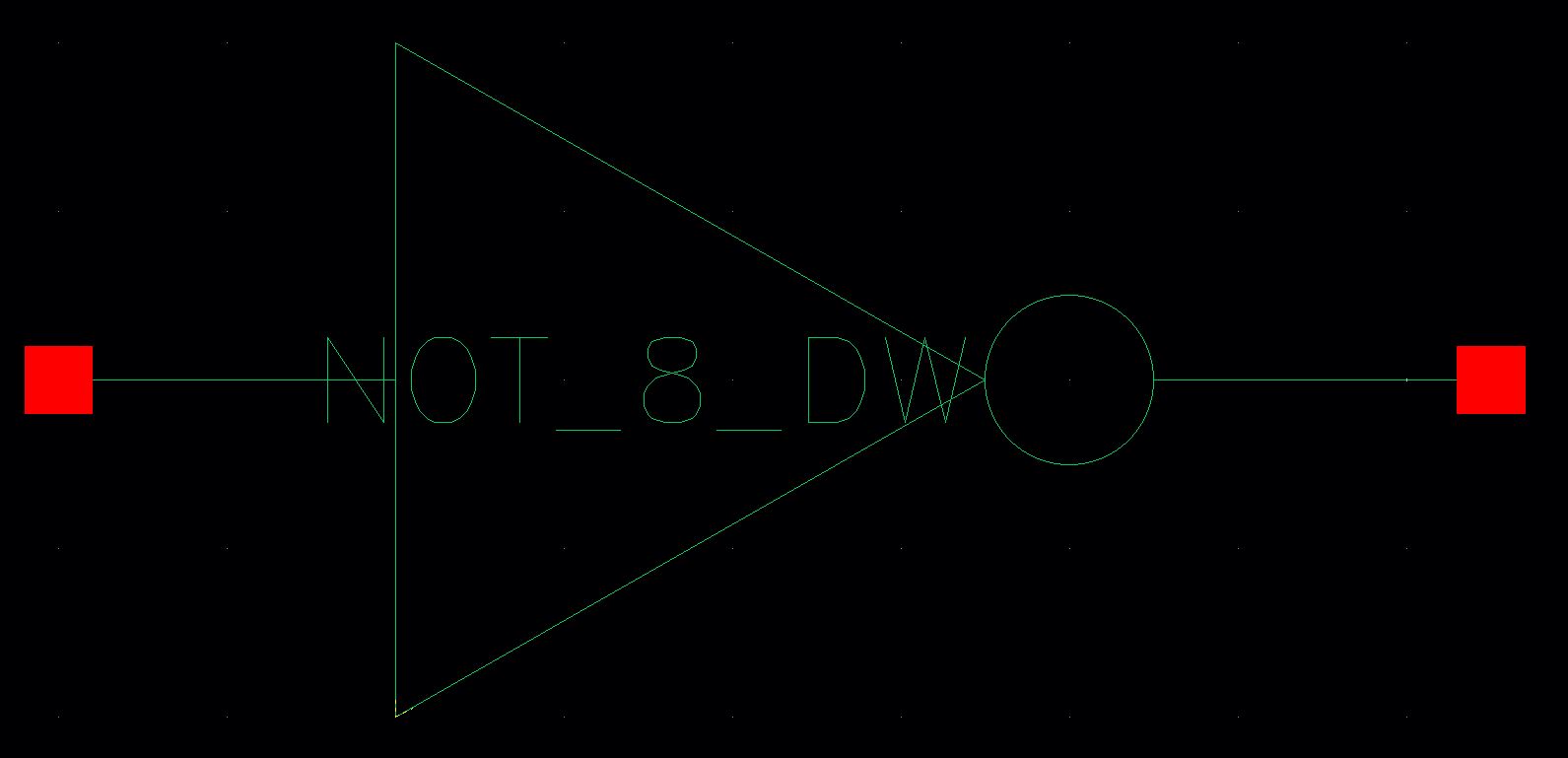
The schematic and symbol for the 8-bit inverter can be seen below:
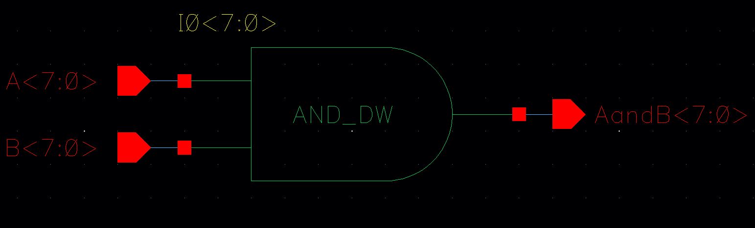
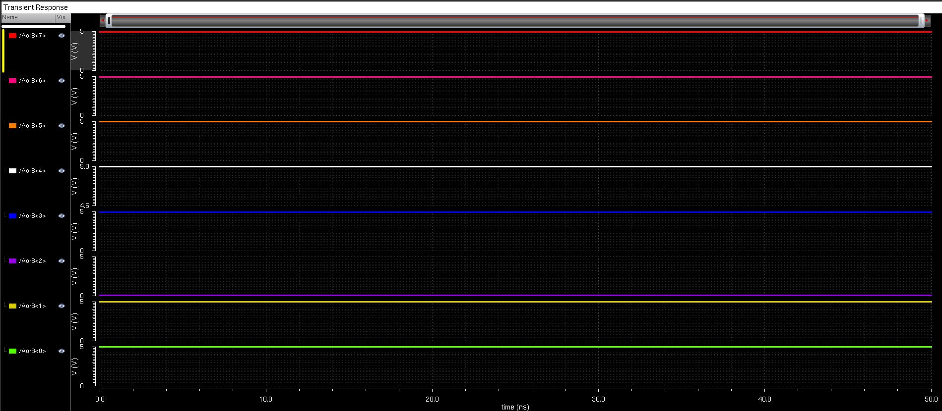
The schematic and results of the simulation for the collection of 8-bit gates can be seen below:
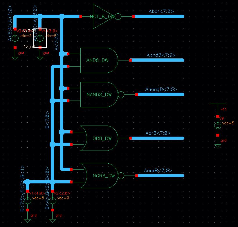
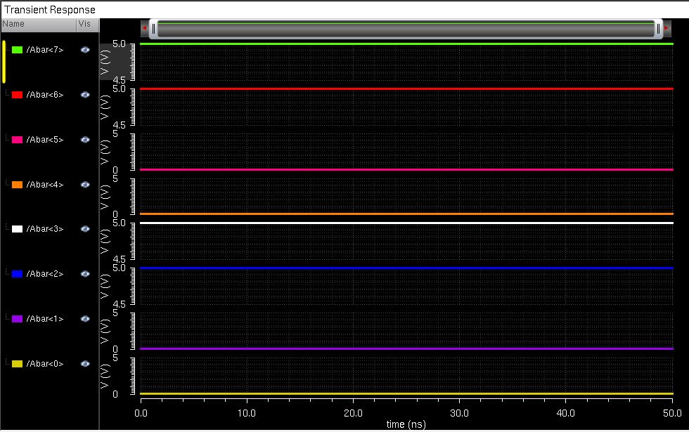
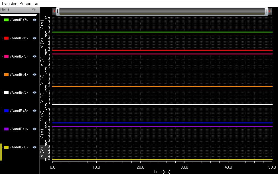
Note that the result of AandB is: 00100010 when A = 00110011 & B = 11101010.
The schematic and symbol for the 2-to-1 MUX/DEMUX is shown below:
Note that this design can work as either a MUX or DEMUX.
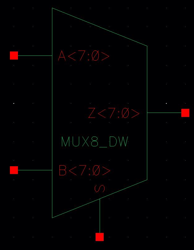
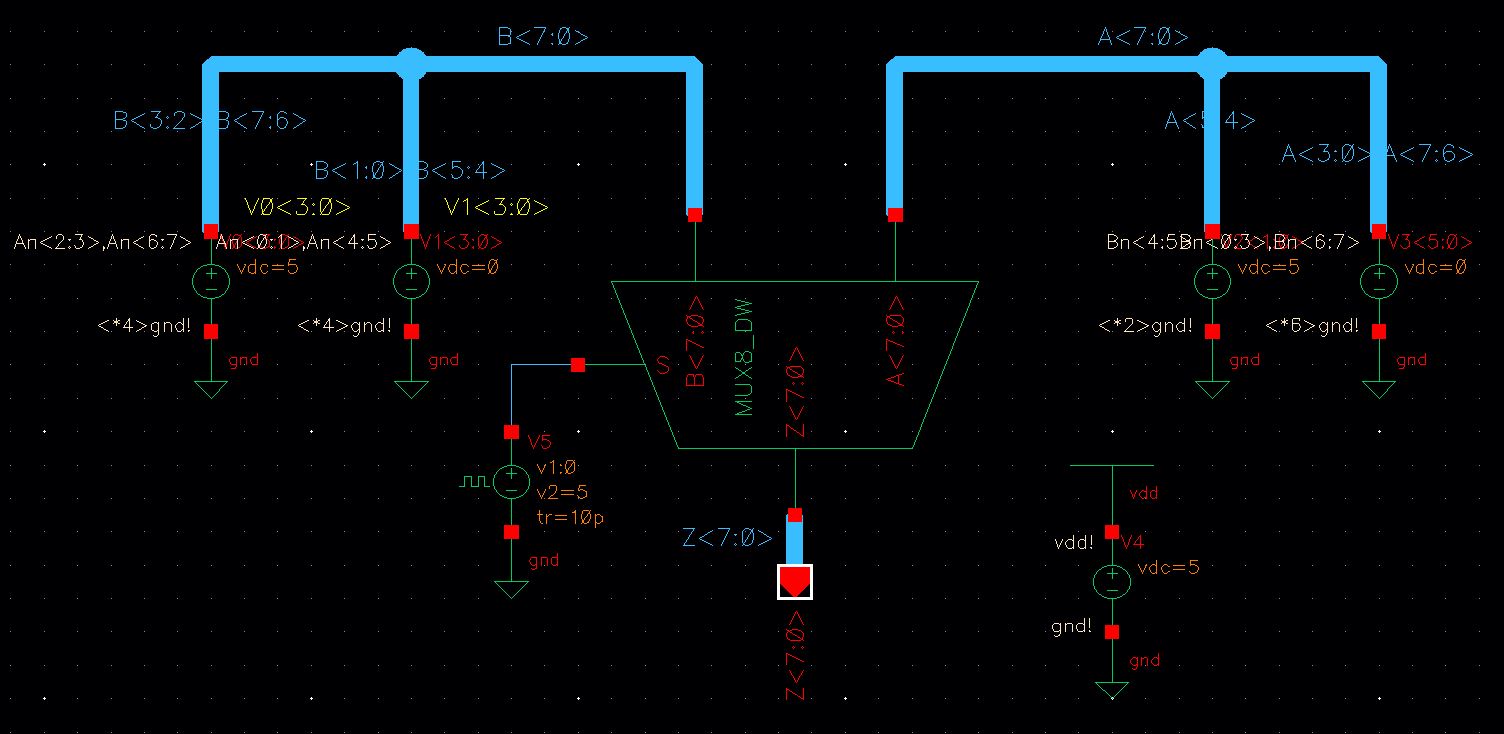
The schematic and symbol for the 8-bit wide MUX is shwon below:
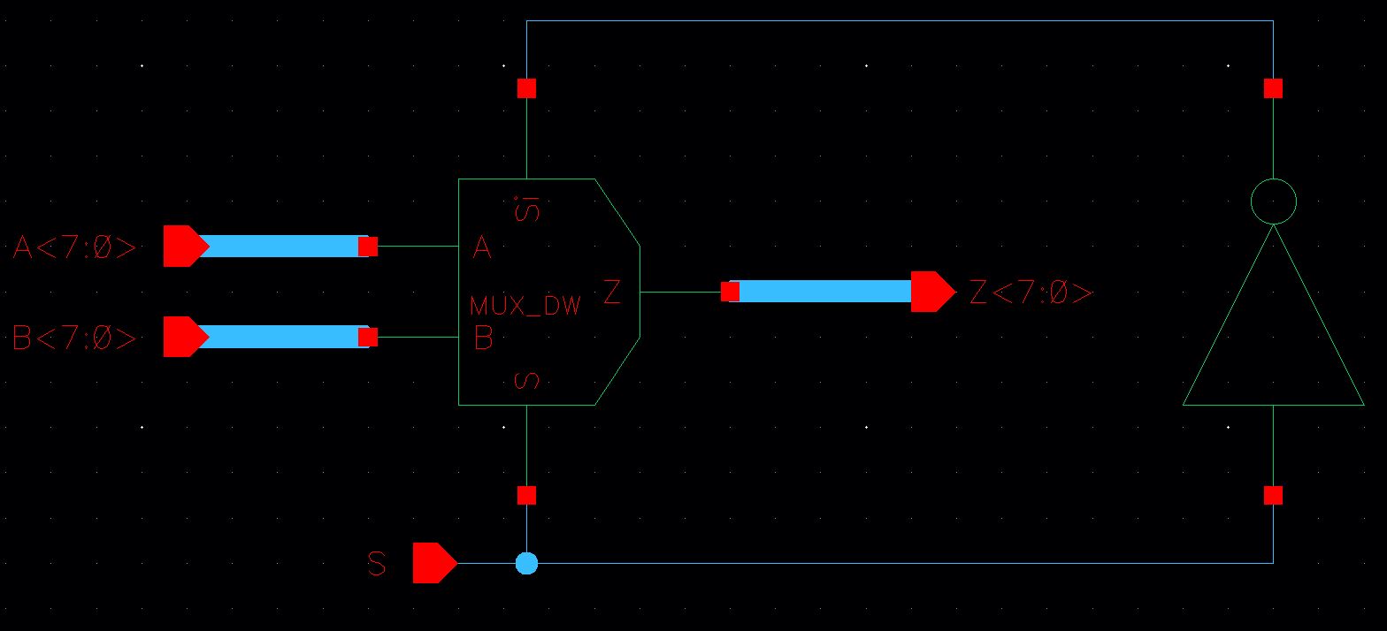
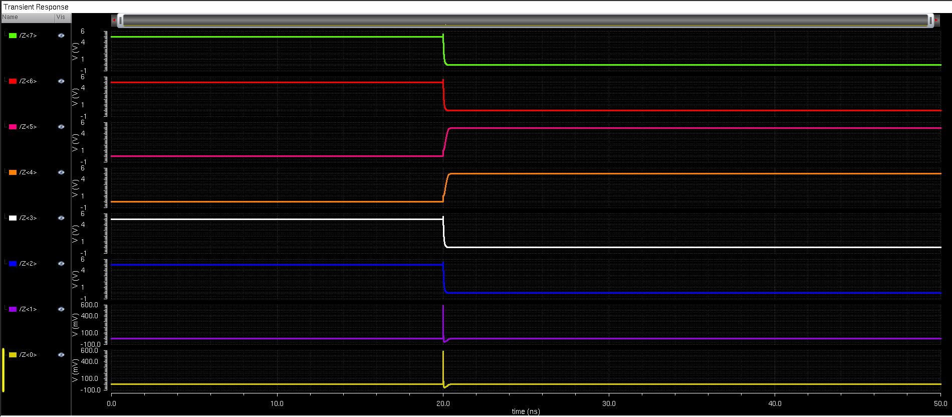
Finally, the simulation schematic and results for the 8-bit MUX choosing between two 8-bit words (A = 00110000 & B = 11001100) using the selection input S:
The schematic, symbol, and layout for the 1-bit Full Adder seen in Fig. 12.20 can be seen below:
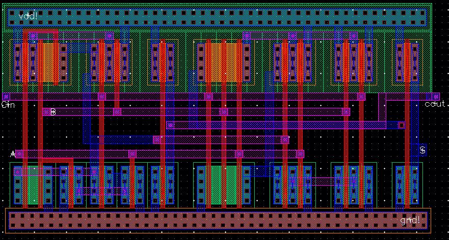
Now, make sure that the layout DRCs and LVSs properly:
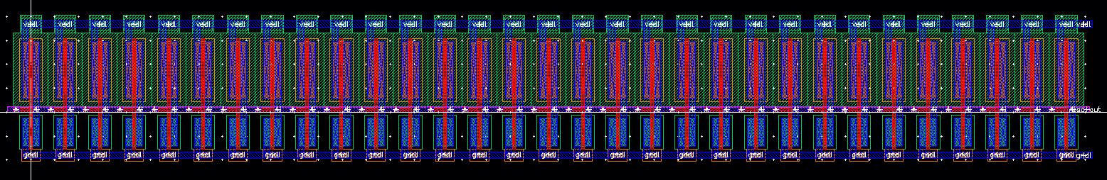
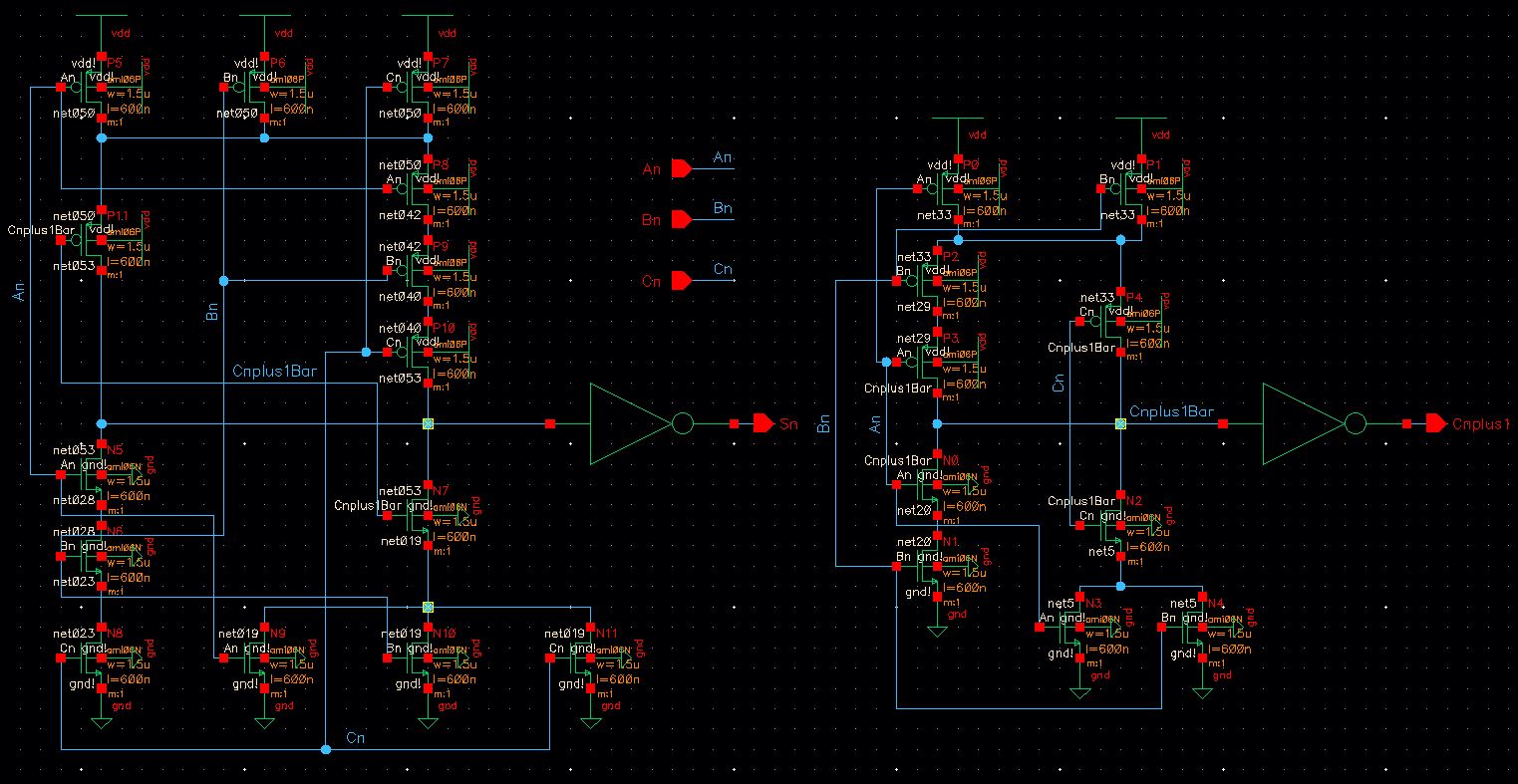
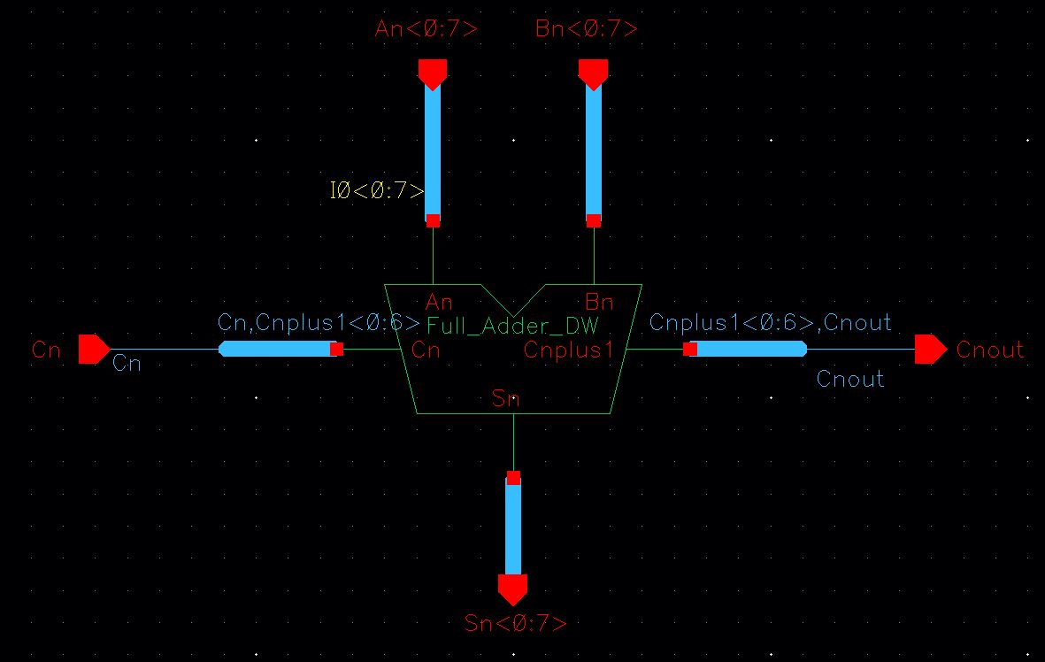
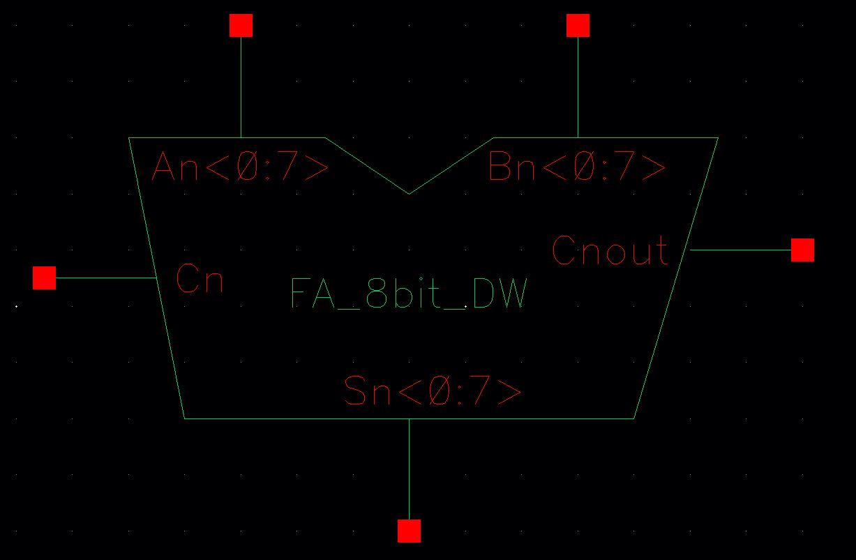
Next, the schematic, symbol, and (quite large) layout for the 8-bit Full Adder can be seen below:

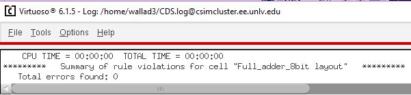
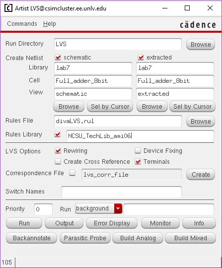
Now, make sure that our large layout is able to DRC and LVS properly (may take awhile):
 `
` 
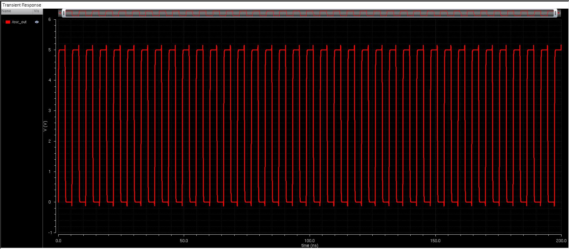
Finally, we can simulate our 8-bit Full-Adder. Below is the schematic of the simulation and the simulation result:
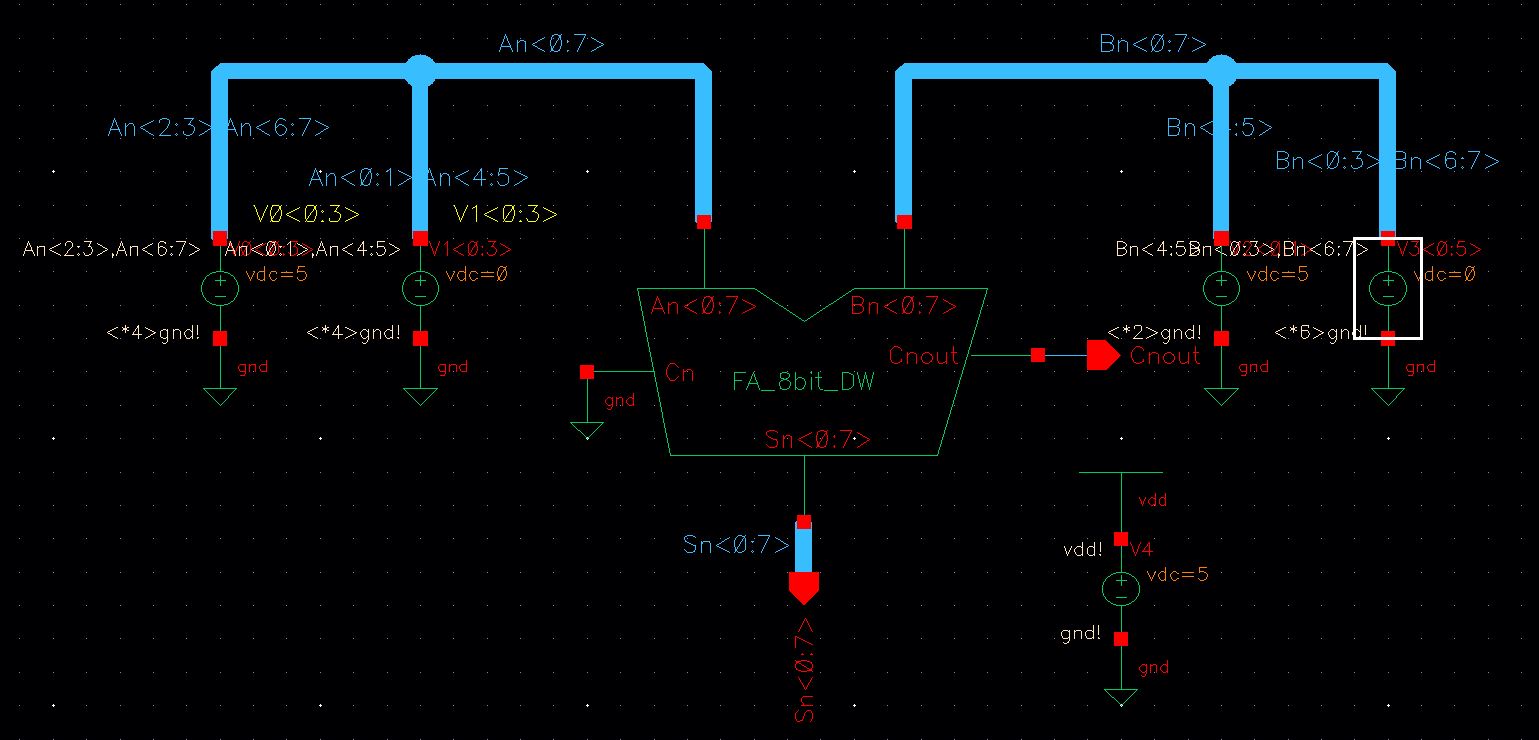
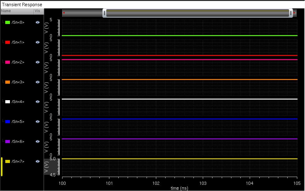
Note that Sn = 00111111 when An = 00110011 & Bn = 00001100.
This concludes the main content for Lab 7.