Finish Tutorial 3.
This ends the content of the Prelab.
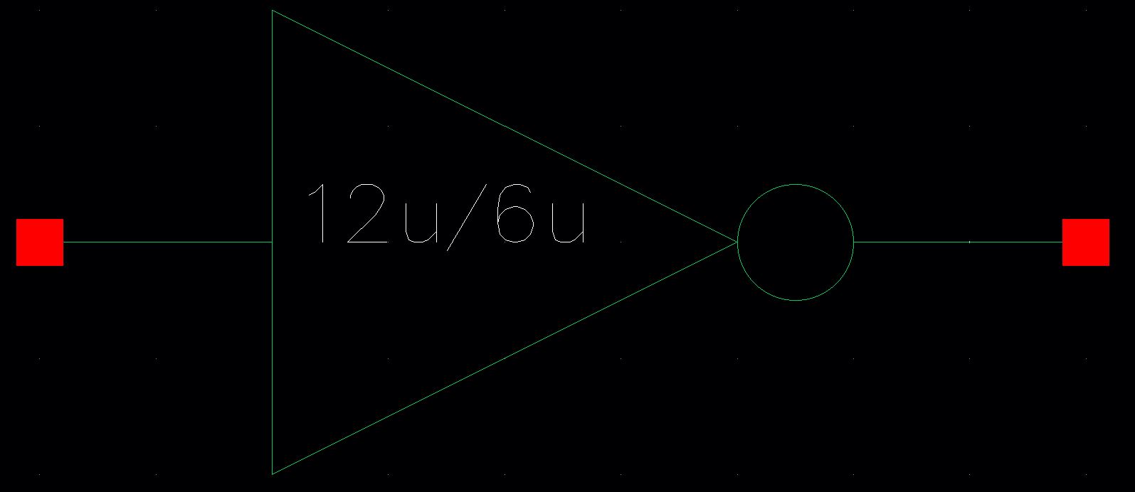
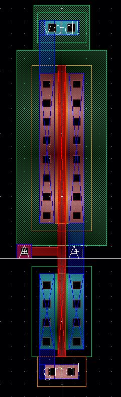
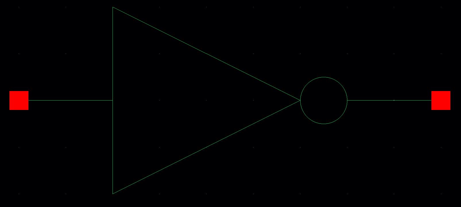
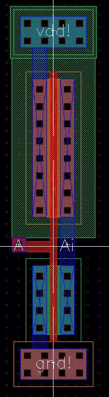
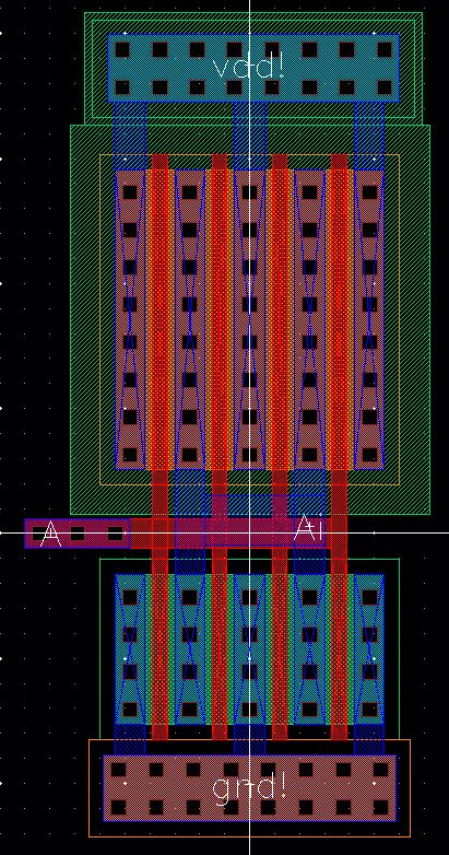
Draft schematics, layouts, and symbols for two inverters having sizes of:
12u/6u (= width of the PMOS / width of the NMOS with both devices having minimum lengths of 0.6u).
48u/24u where the devices use a multiplier, M = 4.
Using SPICE simulate the operation of both of the inverters showing each driving a 100 fF, 1 pF, 10 pF, and 100 pF capacitive load.
Comment, in the report, on the results.
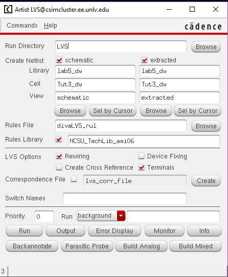
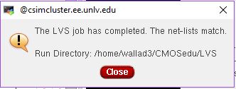
Use UltraSim (Cadence's fast SPICE simulator for larger circuits at the cost of accuracy) and repeat the above simulations.
Zip up these cells in a directory call lab5_dw.zip and link to the lab report.
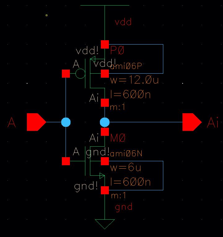
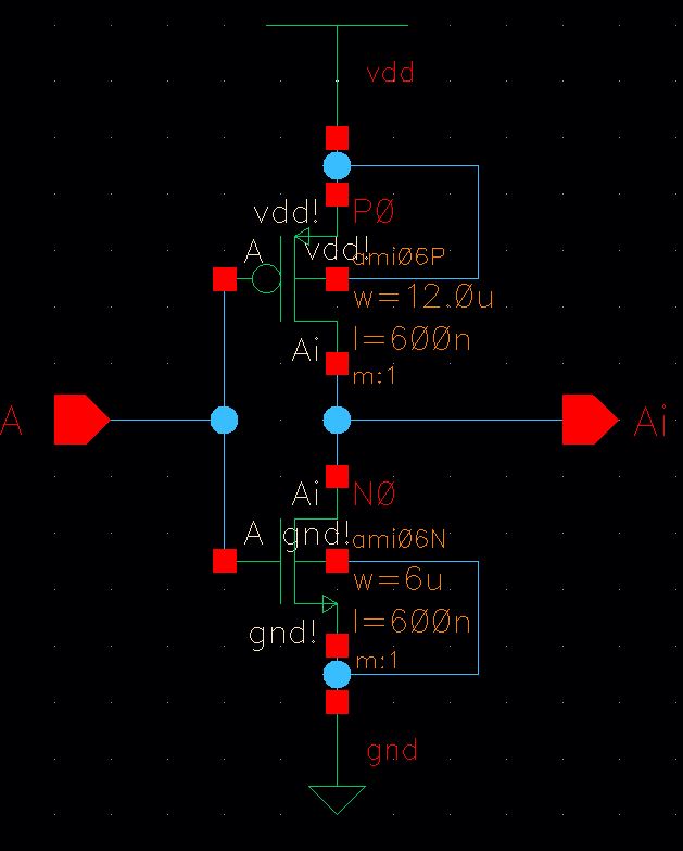
The schematics of the 12u/6u (left) and 48u/24u (right) inverters are shown below:
The symbols representing our schematic are shown below:
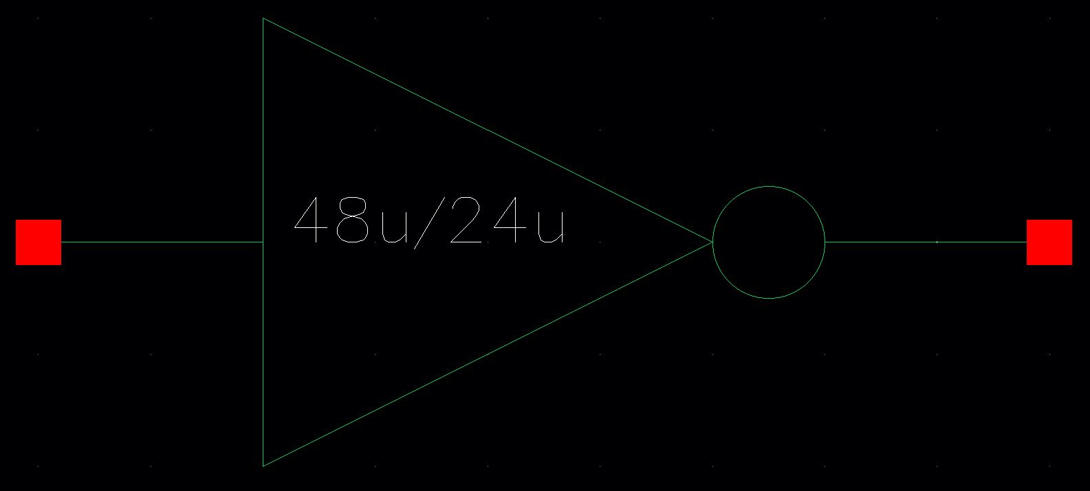
These symbols represent the typical symbol for the NOT gate, which is an inverter.
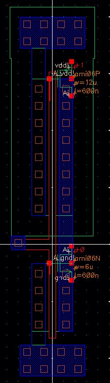
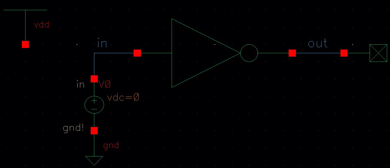
The schematic for the simulation of the 12u/6u inverter is shown below:
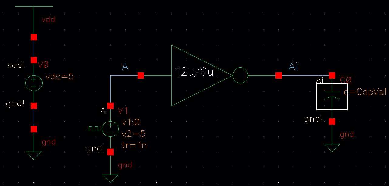
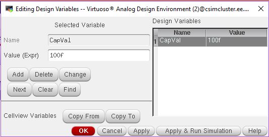
As seen in the image, a variable was used for the capactior value. We will sweep this value by decade from 100fF to 100pF to demonstrate the operation of the CMOS inverter. To acheive this, we will add a variable to the ADE L, as seen below:
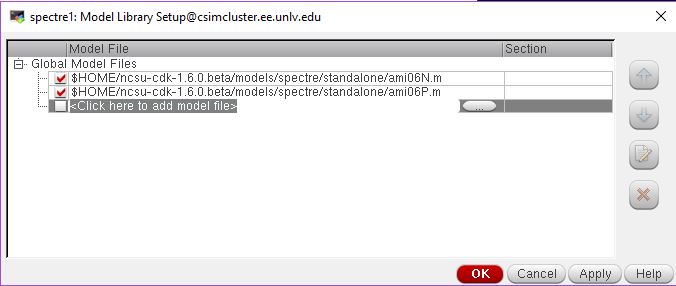
We will run a transient analysis from t = 0 to t = 25 ns. Additionally, we need to add the NMOS and PMOS models to the simulator, as seen below:
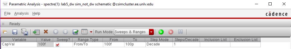
Finally, we can perform a parametric analysis on the CapVal variable, as seen below:
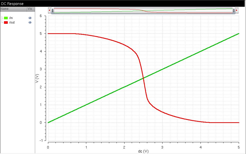
The Spectre results of this analysis can be seen below:
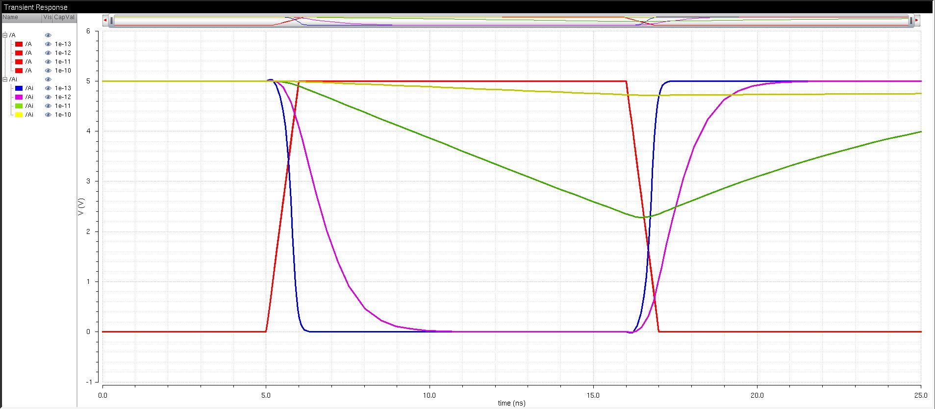
As seen in this image, the coupling capactior reduces the rate of response of the inverter (i.e. the rise/fall time).
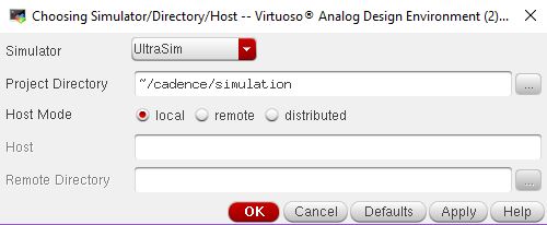
Make sure to save the Spectre state. Now we will run the simulation using UltraSim. Change the simulator by going to Simulator/Directory/Host, and choosing UltraSim, as seen below:
Repeat the steps for adding the models and running the parametric analysis as in the Spectre case. The reults of the UltraSim simulation can be seen below:
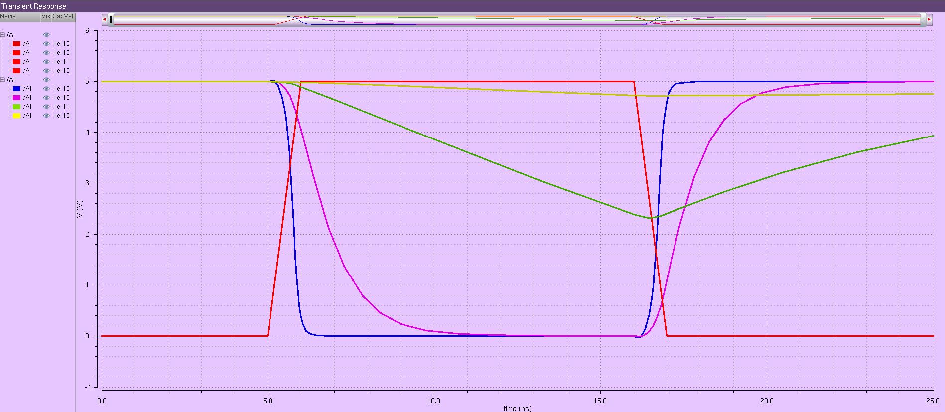
The UltraSim results do run faster than Spectre, but the increased efficiency is not as easily seen as our simulation isn't too large.
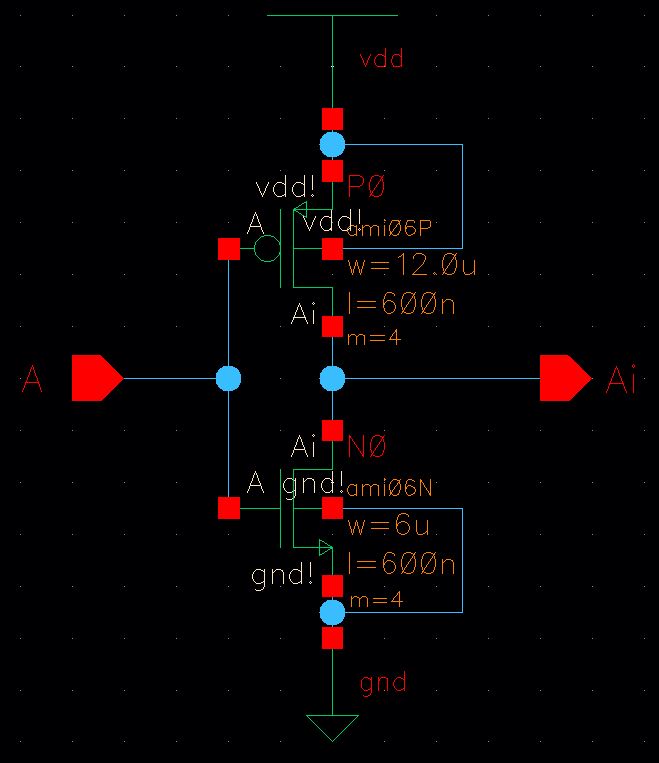
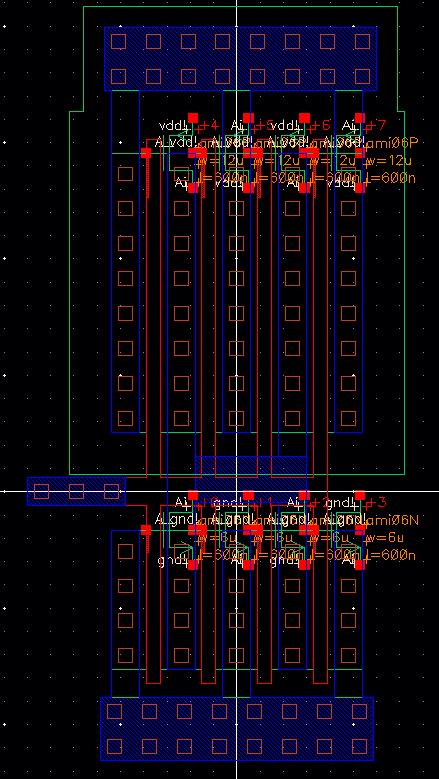
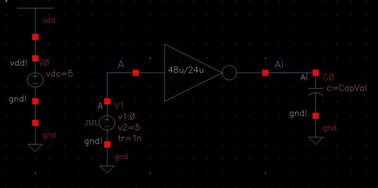
The schematic for the 48u/24u inverter can be seen below:
Again, we will use the CapVal variable to run a parametric analysis. We will repeat the steps for adding the models, variable, and running the parametric analysis. The results of the Spectre simulation can be seen below:
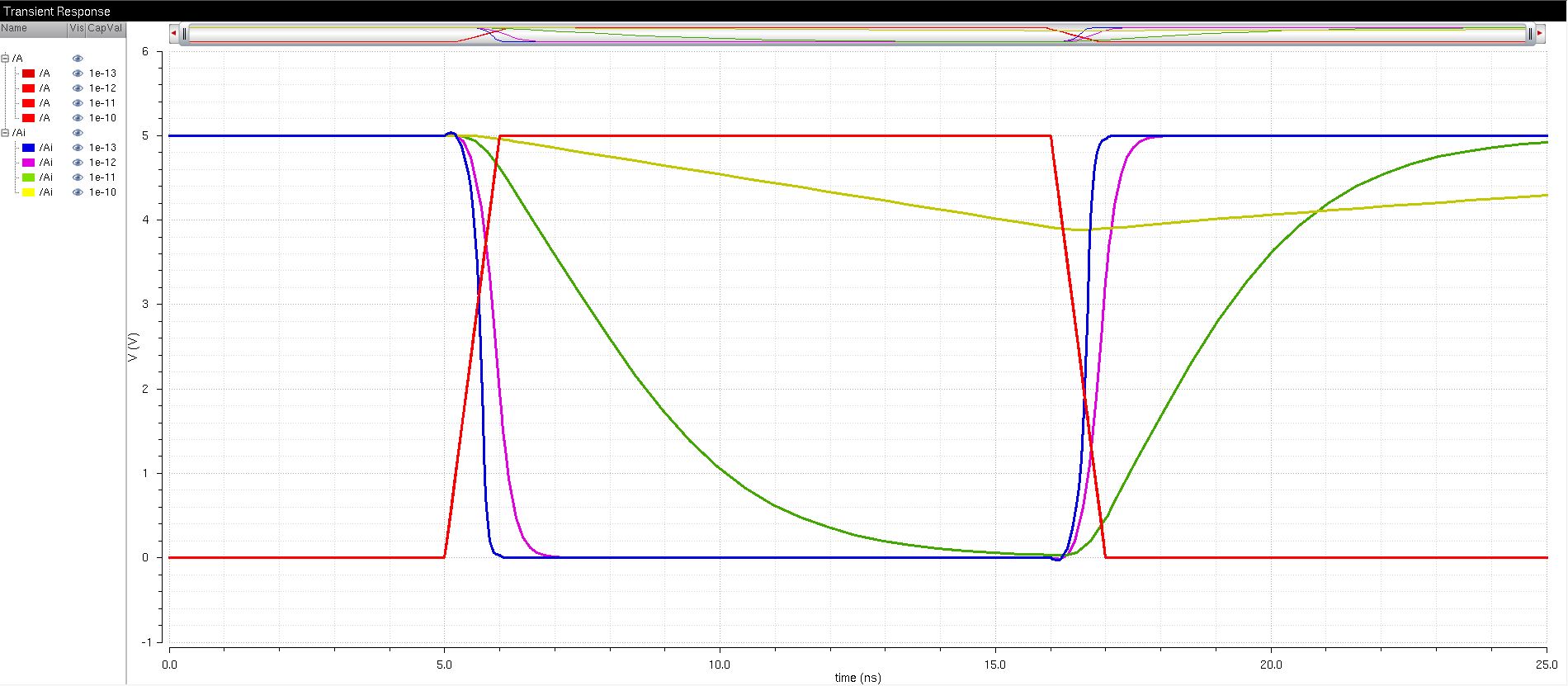
As seen in this image, the effects of the coupling capacitor are reduced with the 48u/24u inverter, due to the increased power output.
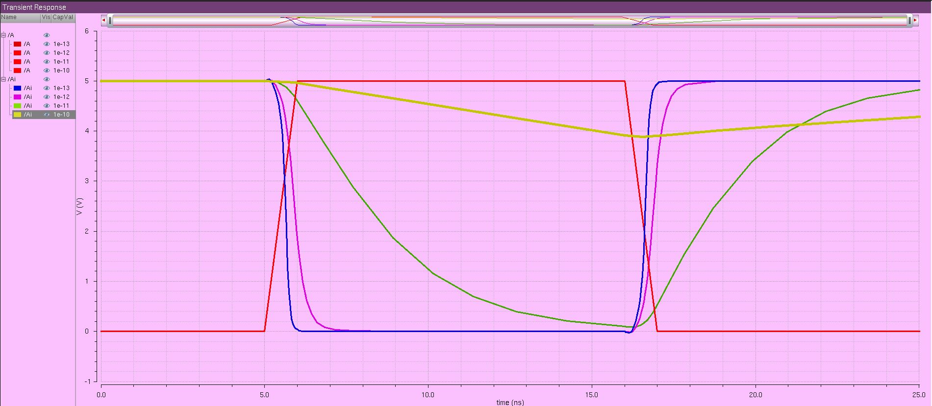
The results for the UltraSim can be seen below:
The zip files for the content of this lab can be accessed here: lab5_dw.zip.
This concludes the main content for Lab 5.