Lab 4 -
EE 421L
Author: Dylan
Wallace
Email: wallad3@unlv.nevada.edu
Date modified:
September 25, 2018
Lab
Description
This lab explores the layout and IV characteristics of NMOS and PMOS devices.
Pre-Lab
objectives
Pre-Lab
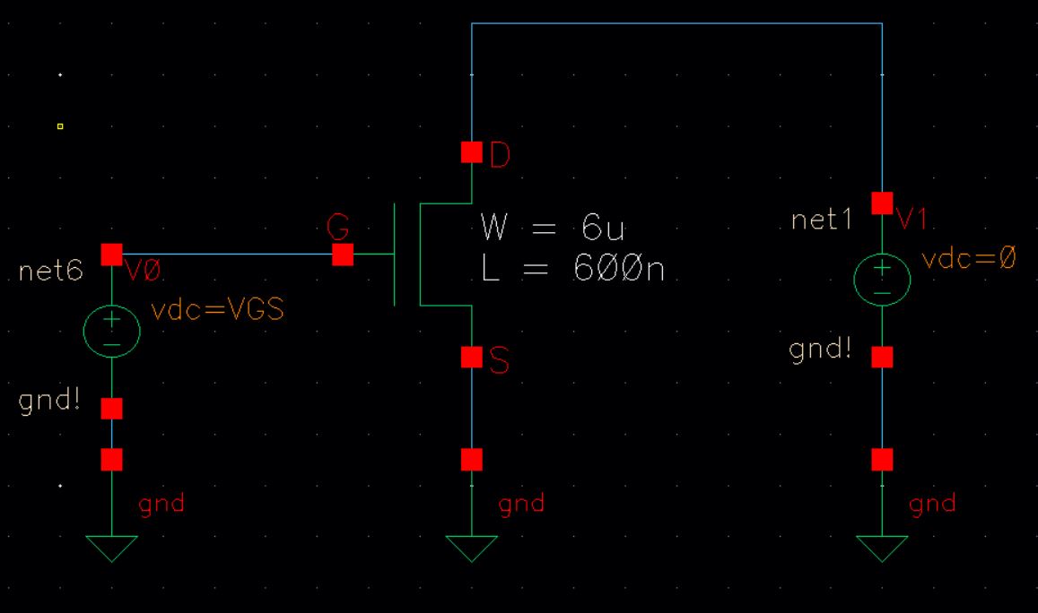
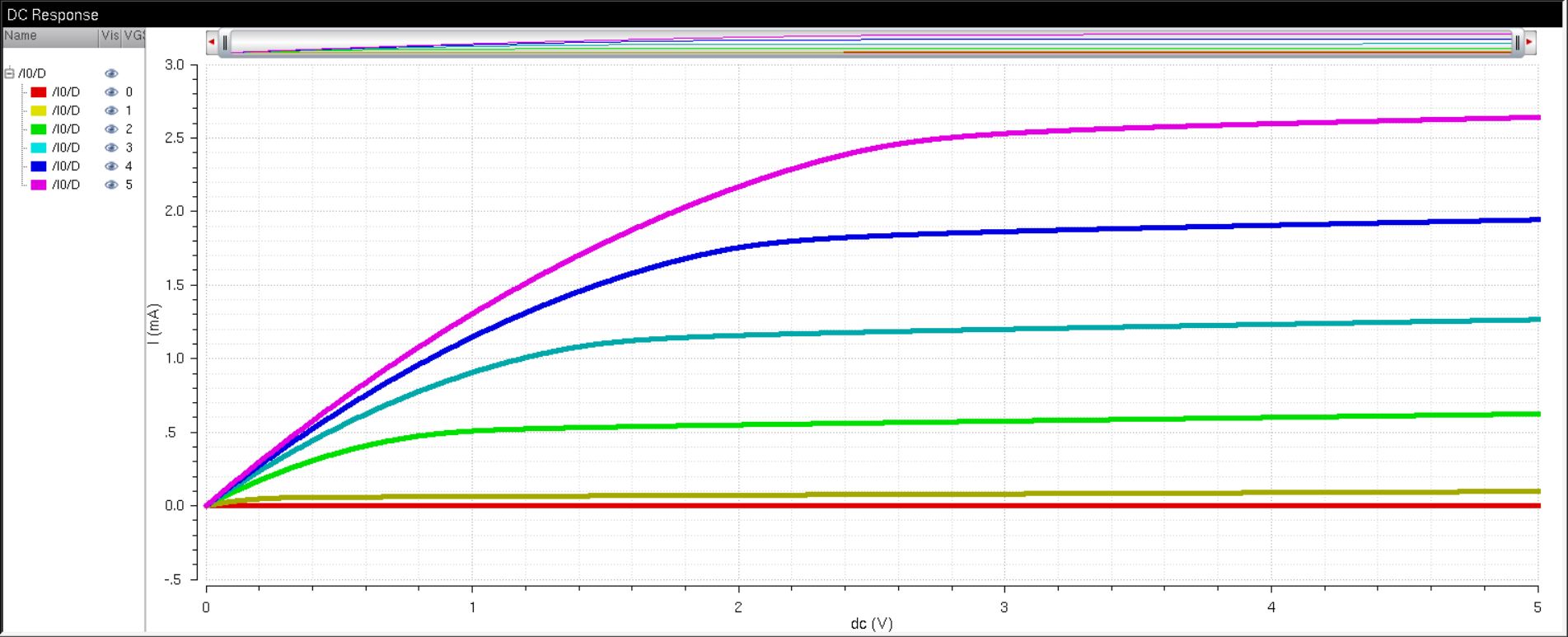
After completing Tutorial 2, you should wind up with the schematic & IV curves seen below:
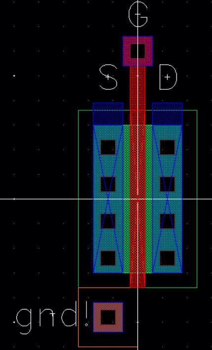
Next you should have layout and extracted views like the images below:
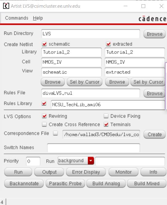
Finally, ensure that the layout LVS's properly as seen below:

This ends the content of the Prelab.
Lab objectives
Lab
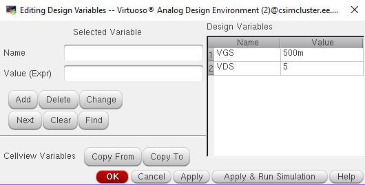
For the following simulation
schematics, we will need to perform a double DC sweep. To perform this,
we must add both sources to be swept in the ADE. This should be done
according to the image below:
Next, we will perform a Parametric Analysis with these variables, according to the image below:
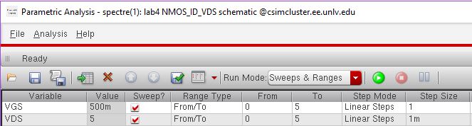
This can be adjusted for each situation to create the desired
effect. Note that for PMOS, the VDS will be changed to VSD and the VGS
will be changed to VSG. NMOS ID v. VDS
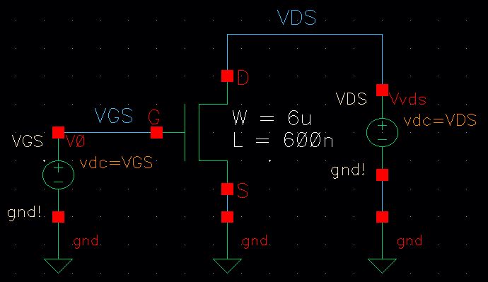
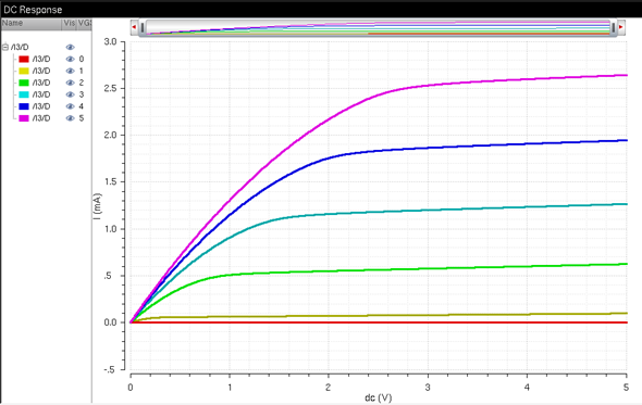
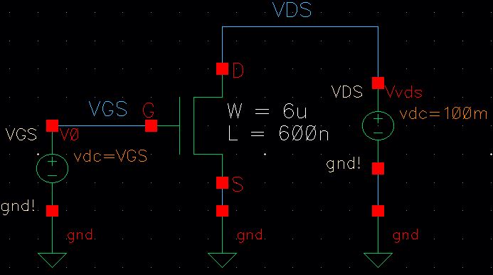
We must create a schematic for simulating ID vs. VDS of an NMOS device for
VGS varying from 0 to 5 V in 1 V steps while VDS varies from 0 to 5 V
in 1 mV steps.
Make sure to use an NMOS with 6u width & 600n
length. The schematic and resulting simulation should look like the
images below:
NMOS ID v. VGS
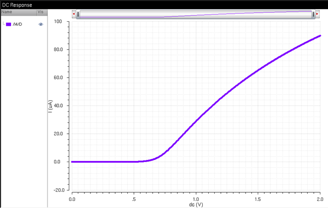
For this simulation, we must create a schematic for
simulating ID v. VGS of an NMOS device for VDS = 100 mV where VGS
varies from 0 to 2 V in 1 mV steps. The resulting schematic &
simulation will look like the images below:
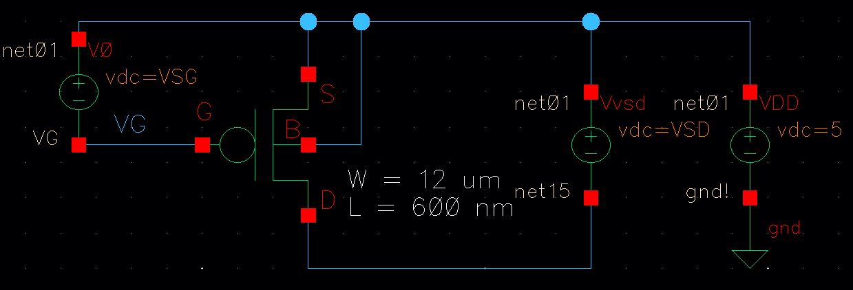
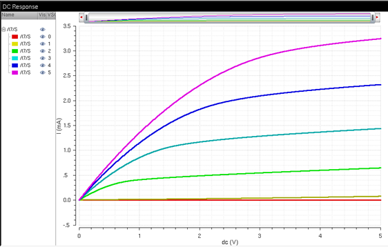
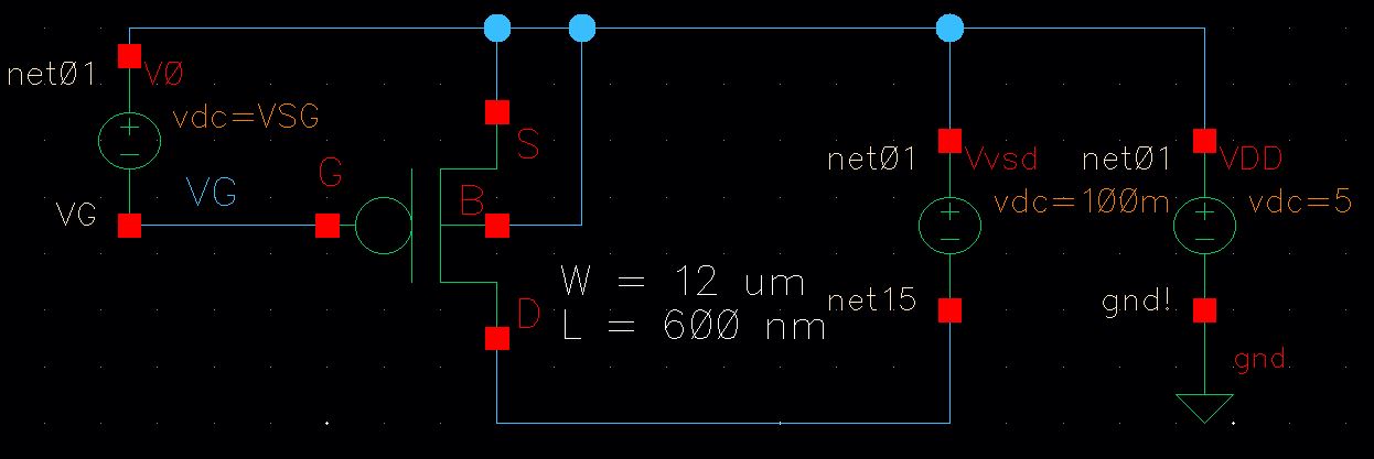
PMOS ID v. VDS
For this simulation, we will create a
schematic for simulating ID v. VSD of a PMOS
device for VSG varying from 0 to 5 V in 1 V steps while VSD
varies from 0 to 5 V in 1 mV steps.
Make sure to use a PMOS with 12u width & 600n length. The schematic
and resulting simulation should look like the images below:
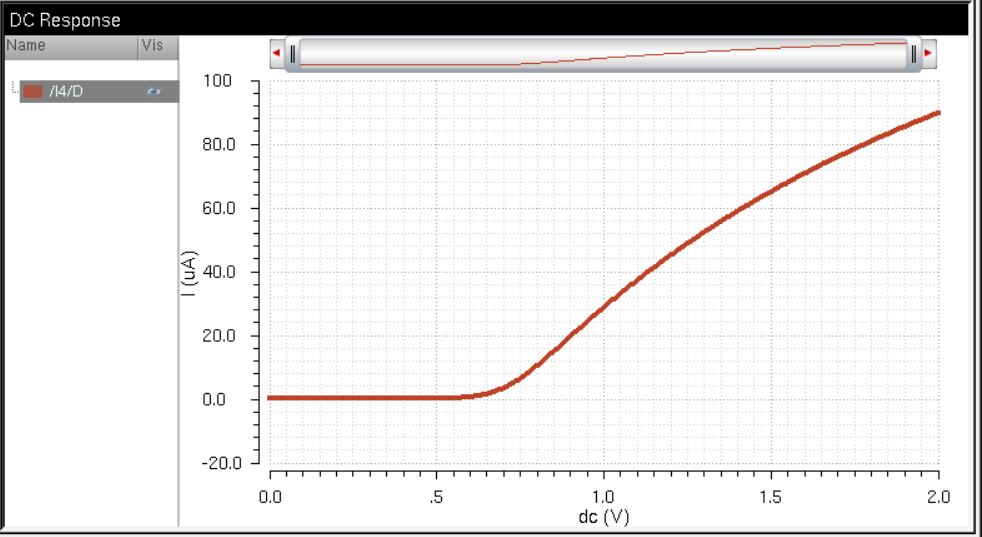
PMOS ID v. VGS
For this simulation, we must create
a schematic for simulating ID v. VSG of a PMOS device for VSD =
100 mV where VSG varies from 0 to 2 V in 1 mV steps. The resulting
schematic & simulation will look like
the images below:
6u/0.6u NMOS device
For this section we will layout the NMOS
device used in the previous simulations. This NMOS will have a width of
6u and a length of 600n. We will connect all four terminals (B, S, D,
G) to Probe Pads which are much smaller than bond pads.
The full schematic should look like the image below:
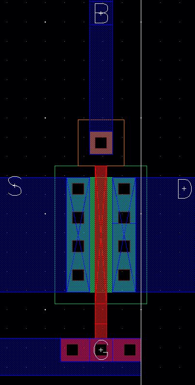
A zoomed in view on the layout of the NMOS
itself can be seen in the image below. Additionally, the output of the
DRC is given below:
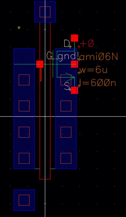
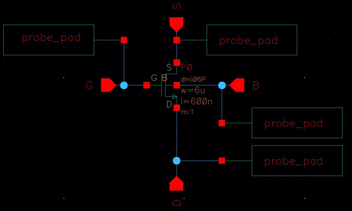
The resulting schematic used for the LVS of the NMOS layout can be seen below:
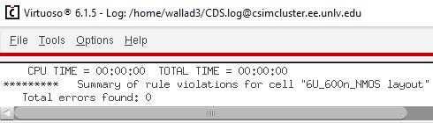
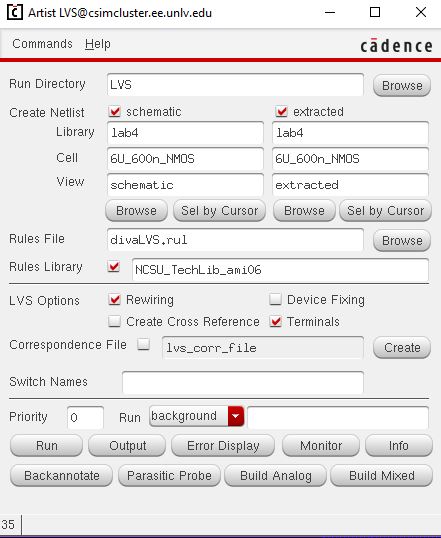
Finally, the LVS setup and output for the NMOS layout can be seen below:

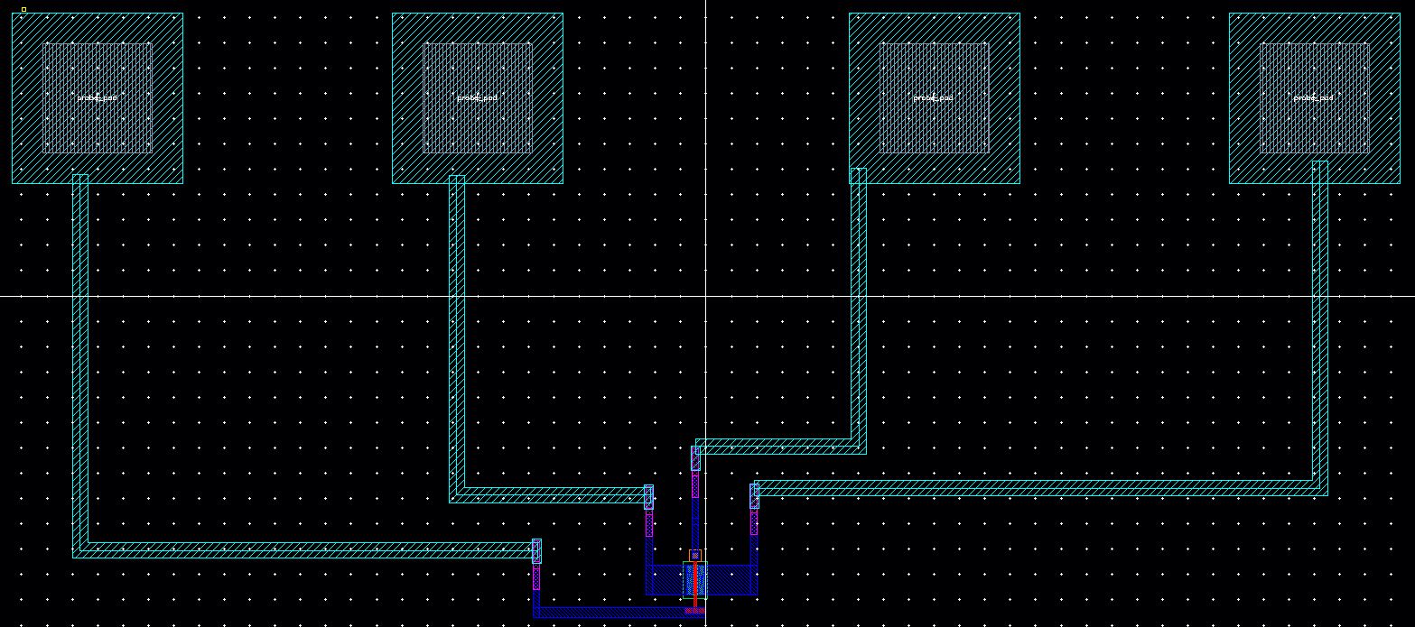
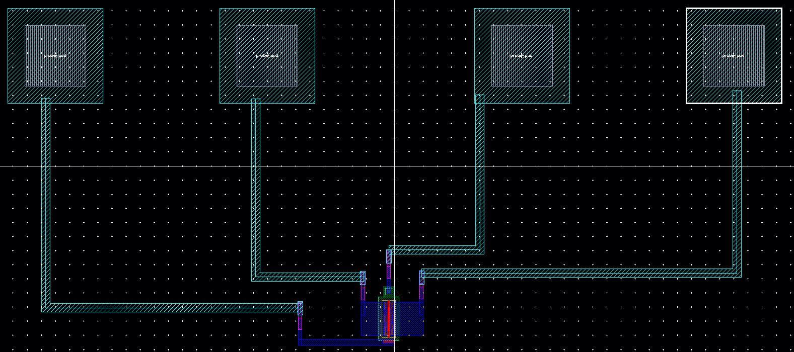
12u/0.6u PMOS device
For this section we will layout the PMOS device used in the previous
simulations. This PMOS will have a width of 12u and a length of 600n. We
will connect all four terminals (B, S, D, G) to Probe Pads which are
much smaller than bond pads. The full schematic should look like the image below:
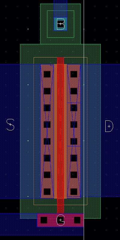
A zoomed in view on the layout of the PMOS itself can be seen in
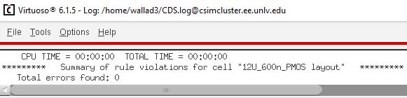
the image below. Additionally, the output of the DRC is given below:
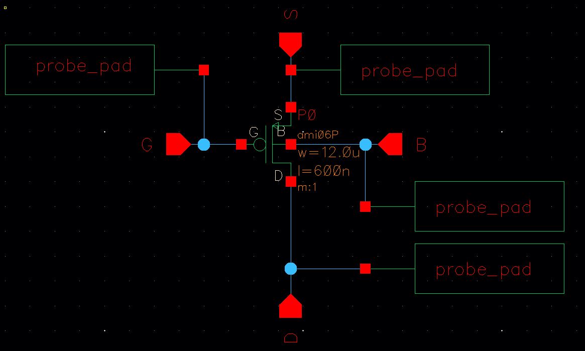
The resulting schematic used for the LVS of the PMOS layout can be seen below:
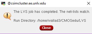
Finally, the LVS setup and output for the PMOS layout can be seen below:
This concludes the main content for Lab 3.
Return to My Labs