Finish Tutorial 1.
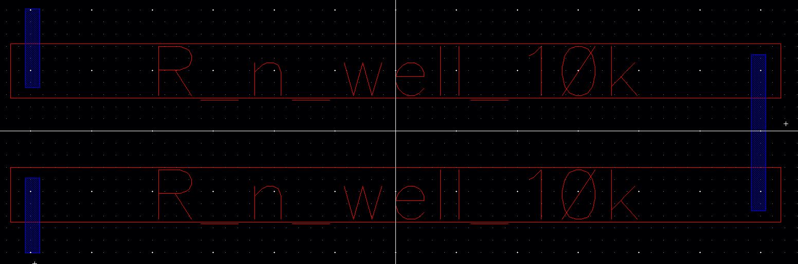
Create a new directory in the "CMOSedu" directory called "lab3" and add the directory to the "cds.lib" file. Copy the "R_n_well_10k" cell to the "lab3" directory using the Library Manager.
This ends the content of the Prelab.
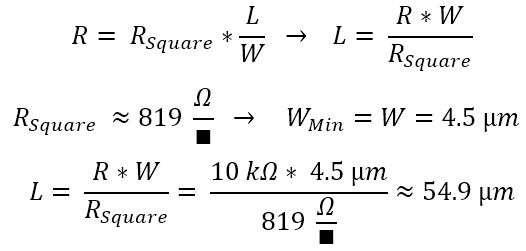
Discuss how to select the width and length of the resistor by referencing the process information from MOSIS.
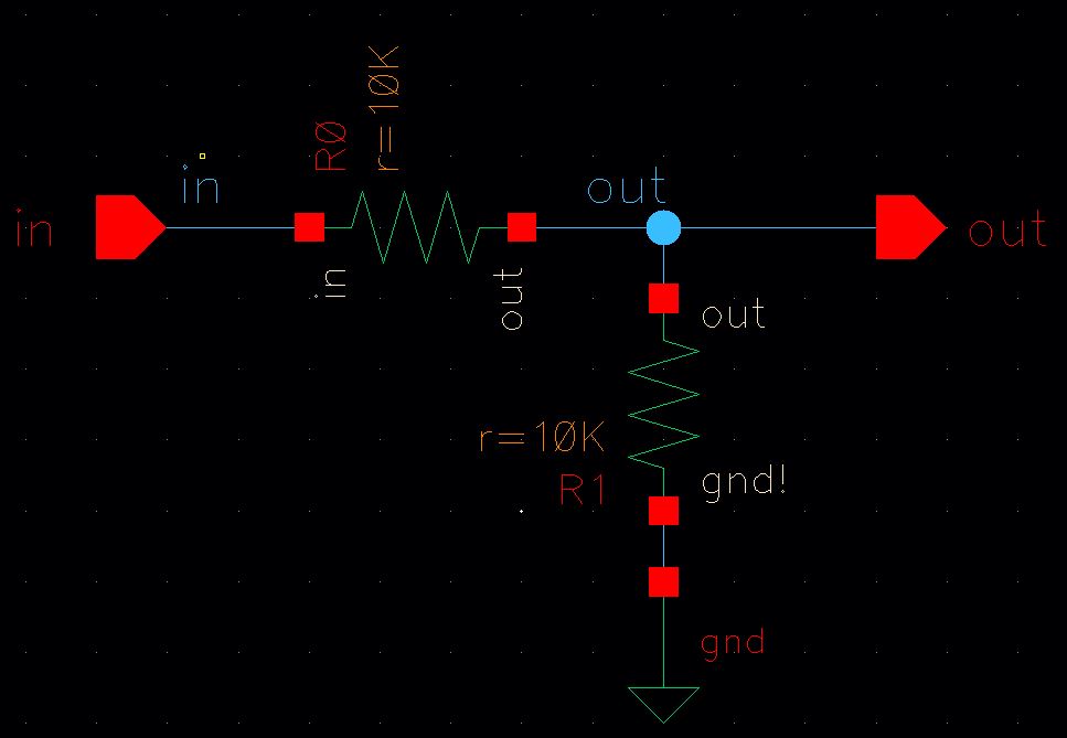
Use the n-well resistor from Tutorial 1 in the layout of the DAC.
DRC and LVS, with the extracted layout, the DAC design.
Zip up the final design directory and place it in the lab3 directory, with a link on the lab report, so the grader can examine both the layout and schematic (and simulations).
The length and width of the n-well can be determined using the equations below:
The width and length of the resistor can be measured by using the Ruler Tool in Cadence.
Simply press "k" in order to activate the Ruler Tool, and choose the first point to measure from. Next, select the second point and the length between the two points will be displayed along the ruler.
Repeat this for both the width and length of the n-well. The layout screen should look like the image below:
Create a new layout in lab3 titled "Lab_10_bit_DAC". First we will take the n-well created in Tutorial 1 and place it into our layout. We will then place another one above the first.
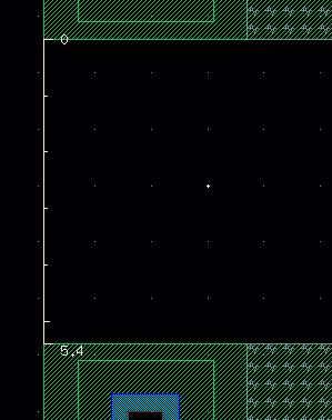
We must make sure that the n-wells are at least 5.4 um apart, so we will measure this with the Ruler Tool as seen below:
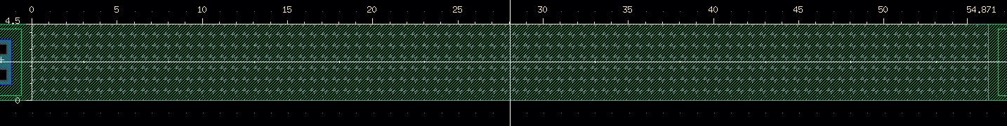
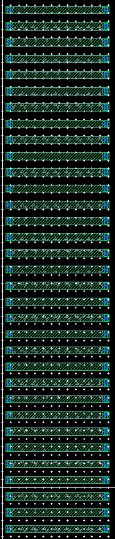
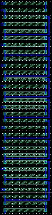
Now we will copy these pairs of n-wells 16 times to create a total of 32 n-wells aligned vertically, as seen below:
Now we will create metal connections between N-wells. First select the "metal_1" layer, and then press "r" to create a rectangle. Connect the N-wells as seen below, and add pins "B0" and "gnd".
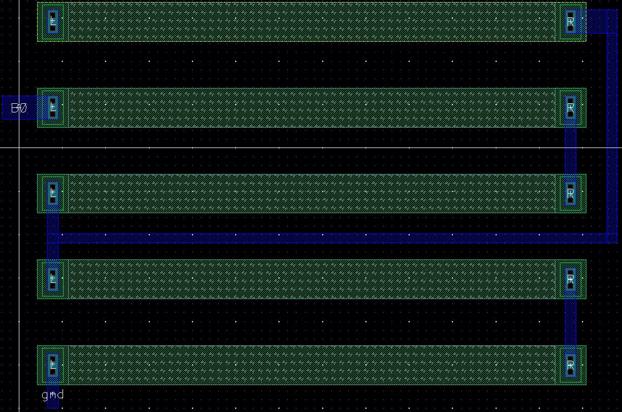
Now copy this layout all the way up the DAC until the top. Be sure to add pins "B1" through "B8". The top of the DAC should look like the image below. Be sure to add the pins for "B9" and "Vout".
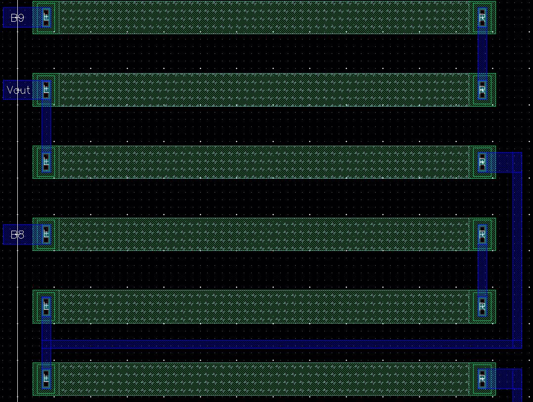
The final layout of the 10-bit DAC should look like the image below:
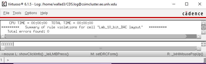
DRC the layout to make sure that no errors were made. The Command Window should look like below:
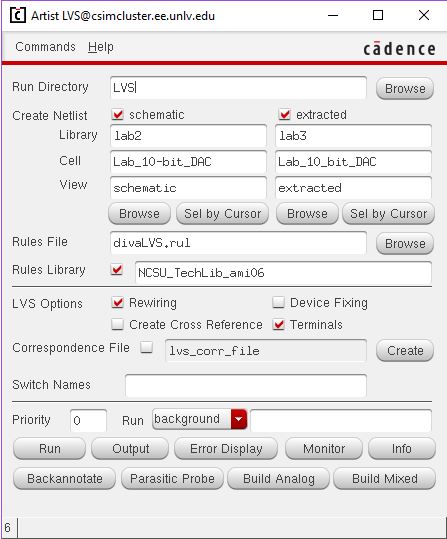
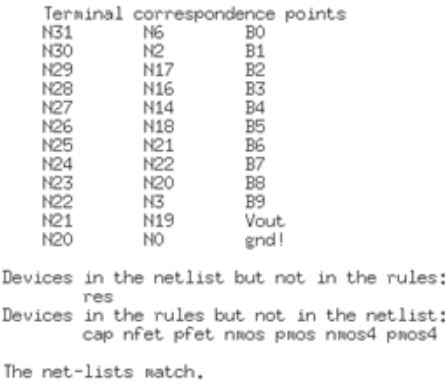
Now we must LVS the layout to make sure that it matches our schematic. First, we will extract the layout view by going to "Verify -> Extract..." and pressing "OK". Now go to "Verify -> LVS..." and configure your window to look like below:
The output of the LVS should look like below:
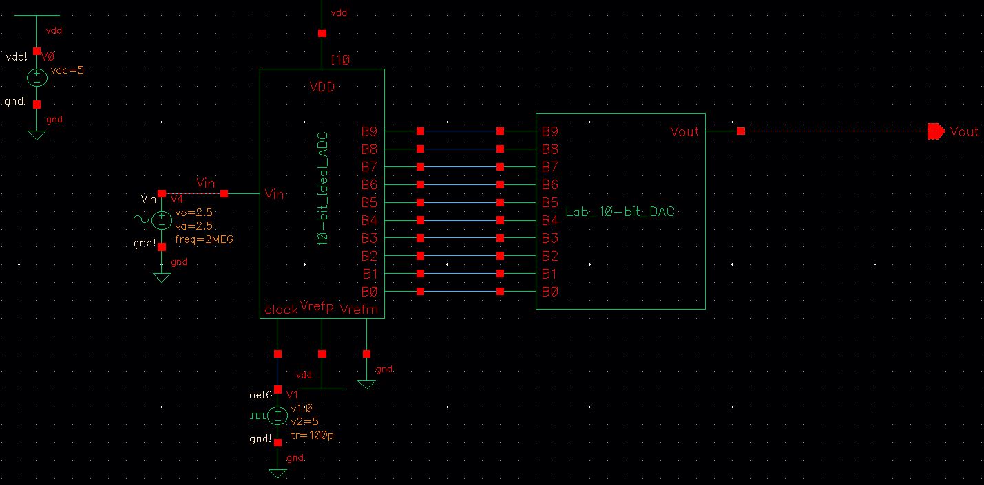
Next, we will create a symbol for our layout and add it to the 10-bit ADC-DAC schematic. Delete the Ideal 10-bit DAC and replace it with the symbol that you just created. The schematic should look like below:
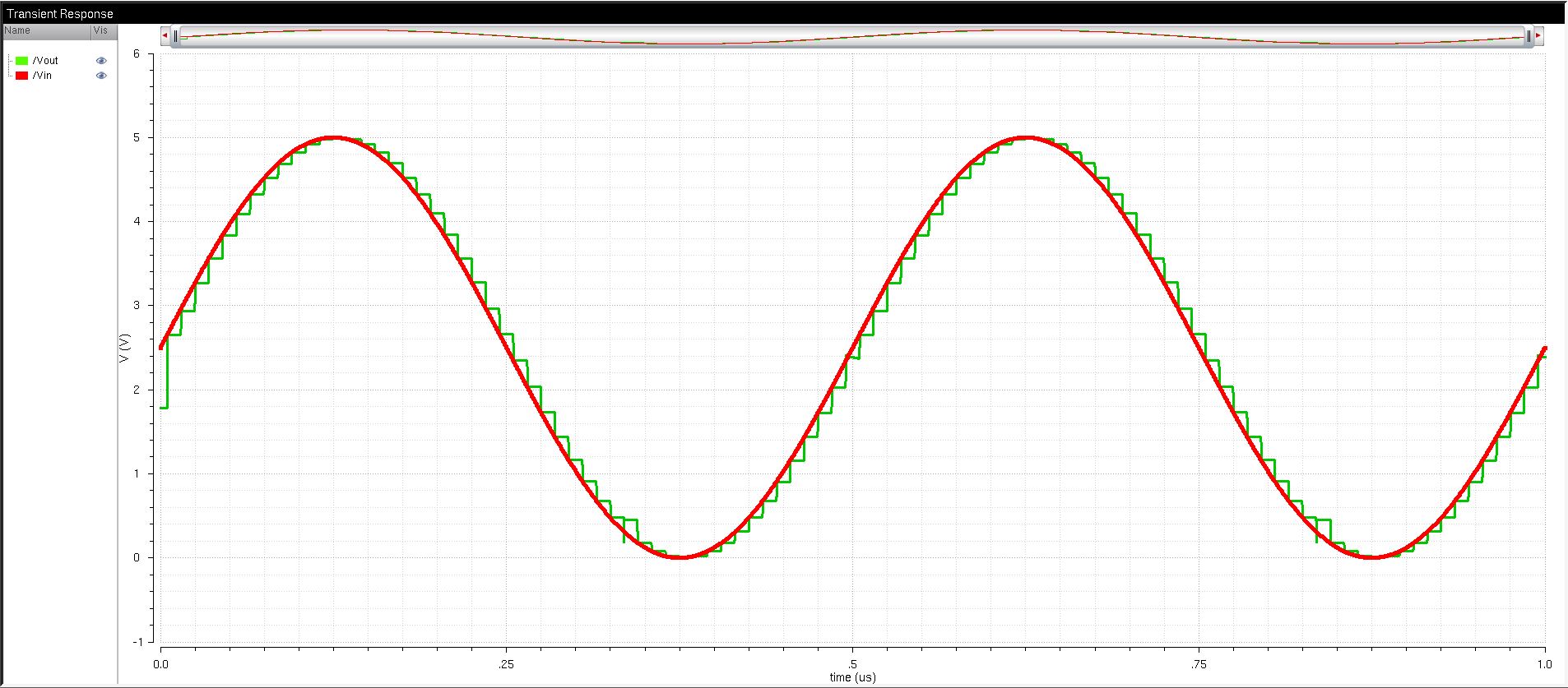
Finally, launch ADE L and load the spectre_state for the schematic. Simulate the schematic and change the properties of the graph to look like the image below:
The files used in Lab 3 can be found in lab3.zip.
This concludes the main content for Lab 3.