Lab 8 - EE 421L - Digital Integrated Circuit Design
Generate a test chip layout for submission to MOSIS for fabrication
| Chip Schematic | Chip Layout |
| |
| Symbol | How to test |
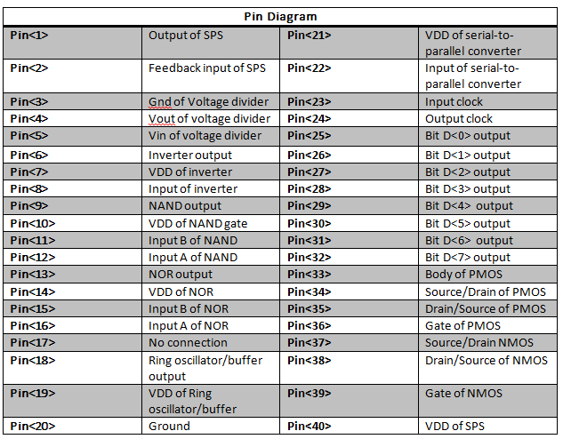
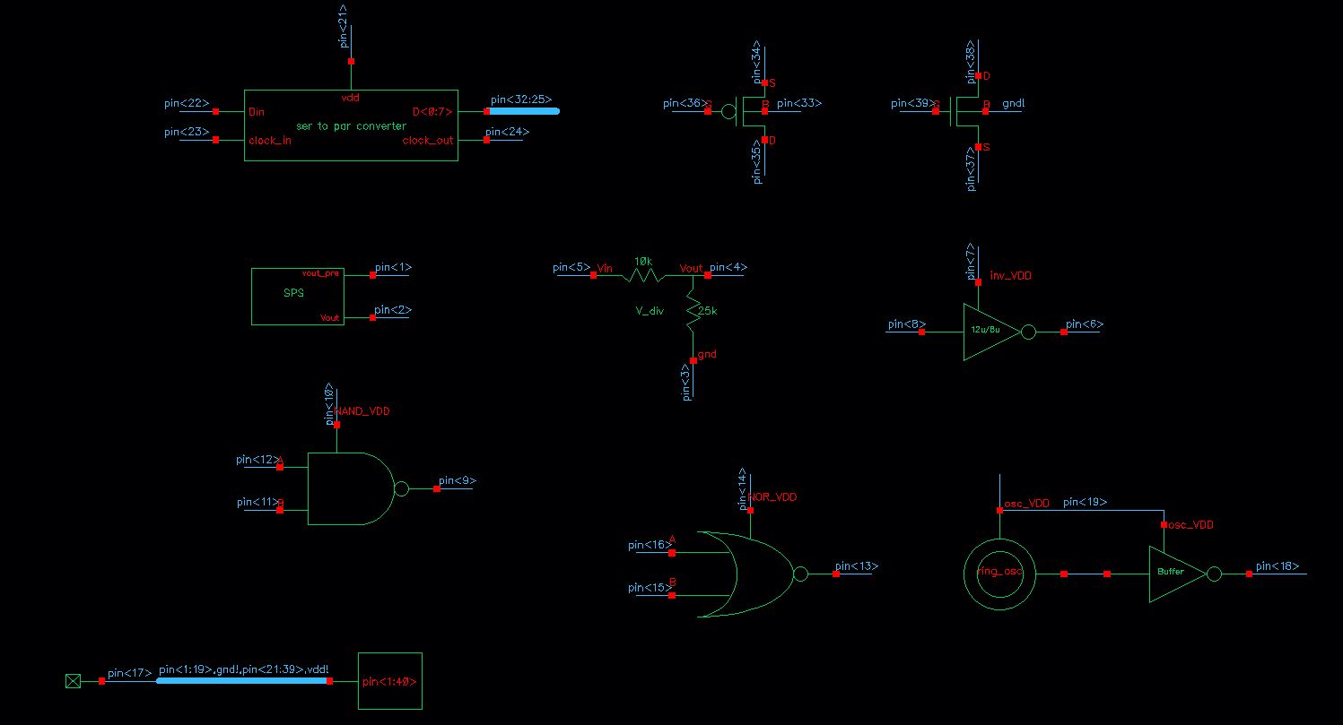
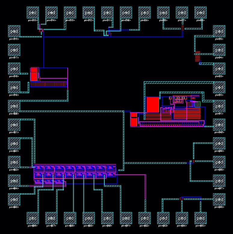
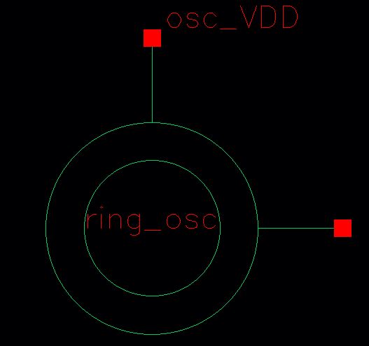 | Ground pin<20> Connect 5V VDD to pin<19> Measure the output at pin<18> The output of the ring oscillator is connected to a buffer composed of three inverters with gain(A) = 8 in order to drive a 20pF off-chip load. The ouput of the buffer is pin<18> is |
| Symbol | How to test |
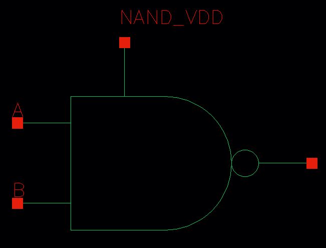 | Ground pin<20> Connect 5V VDD to pin<10> Apply inputs to pin<11> and pin<12> Measure the output at pin<9> |
| Symbol | How to test |
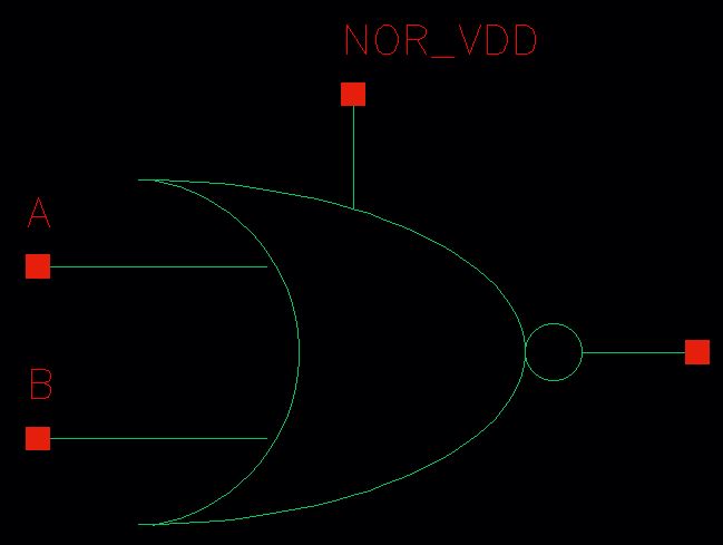 | Ground pin<20> Connect 5V VDD to pin<14> Apply inputs to pin<15> and pin<16> Measure the output at pin<13> |
| Symbol | How to test |
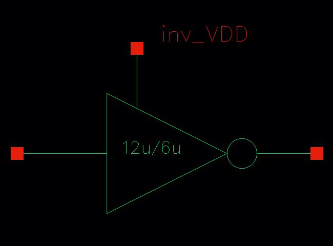 | Ground pin<20> Connect 5V VDD to pin<7> Apply input to pin<8> Measure the output at pin<6> |
| Symbol | How to test |
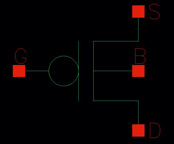 | Apply 5V VDD to body at pin<33> Drain connection at pin<35> Source connection at pin<34> Gate input at pin<36> |
| Symbol | How to test |
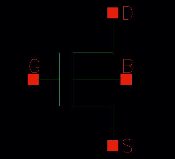 | Ground the body at pin<20> Drain connection at pin<38> Source connection at pin<37> Gate input at pin<390--> |
| Symbol | How to test |
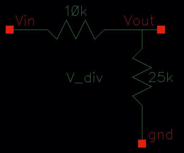 | Ground pin<3> Apply Vin at pin<5> Measure Vout at pin<4> |
| Symbol | How to test |
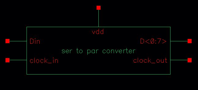 | Ground pin<20> Apply 5V VDD to pin<21> Apply input to pin<22> Apply input clock to pin<23> Measure the outputs at pin<25:32>, these are the parrallel output of the system. Measure the clock out at pin<24>, this output clock is the input clock signal devided by 8 or decresed by eight times. |
| Symbol | How to test |
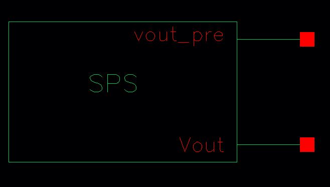 | Ground pin<20> Measure the output of the SPS at pin<1>. This pin connect to an 30uH inductor and to a schottky diode. The inductor is connected to VDD on the other side. The other side of the diode is connected to a 5uF capacitor and a 250 Ohm resistor (load). The node connected to the capacitor and load resistor is Vout and is used as the feedback into the system of the SPS. This circuit composes a Boost SPS. This set up works with a VDD range of 3.74V to 4.75V, to maintain 5V at the Vout node. Measure the feedback input at pin<2> This pin has label Vout |