Lab 7 - EE 421L: Using buses and arrays in the design of word inverters, muxes, and high-speed adders
Email: matacarl@unlv.nevada.edu
Pre-lab:
Back-up
all work from the lab and the course
Finished
Tutorial 5 seen here.
And
read through the lab prior to class
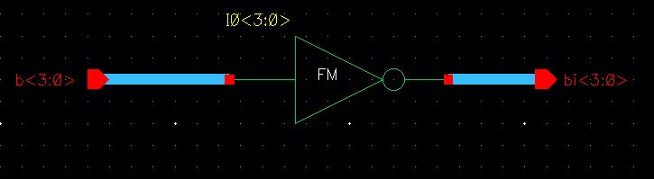
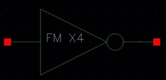
4-bit
word inverter schematic and symbol
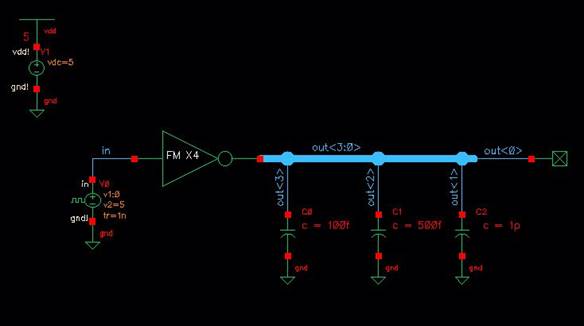
Below
is the 4-bit word inverter simulation with different loads; 100fF, 500fF, 1pF,
and no load
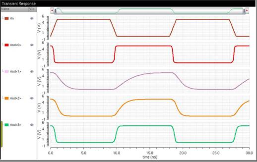
From
the plot above we can see that as the capacitance of the load increases the
rise time and the fall time increases due to the RC time.
|
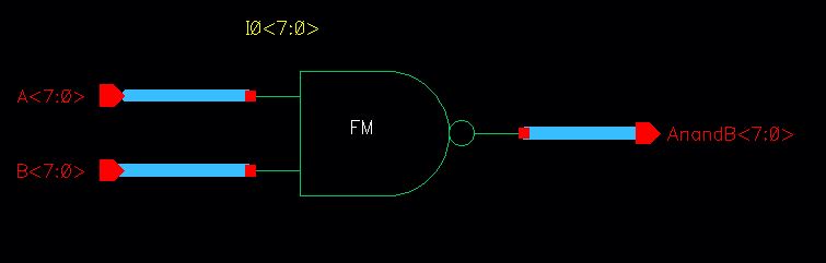
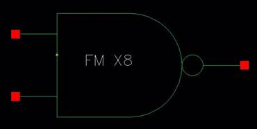
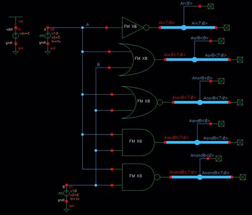
8-bit NAND gate schematic and symbol |
|
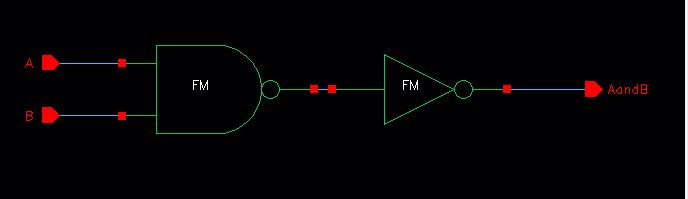
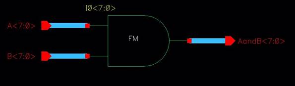
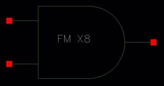
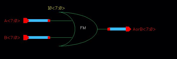
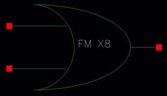
8-bit AND gate schematic and symbol.
This gate was made using the NAND gate from previous lab with an inverter.
|
|
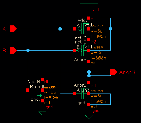
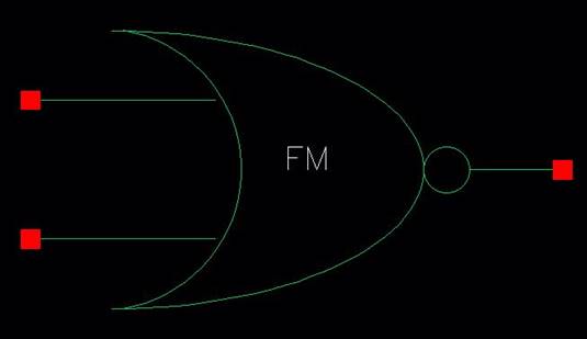
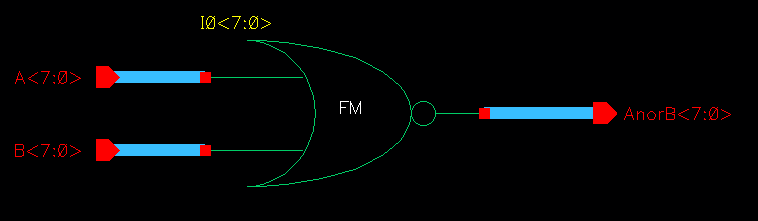
8-bit NOR gate schematic and symbol
|
|
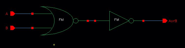
8-bit OR gate schematic and symbol.
This gate was made using the NOR gate with an inverter.
|
|
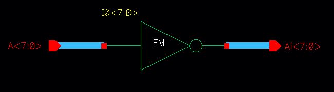
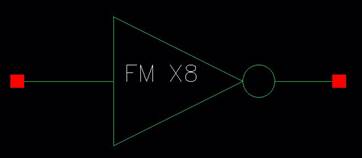
8-bit inverter schematic and symbol
|
Below
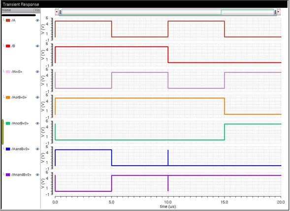
are the schematic and simulation for the logic gates above
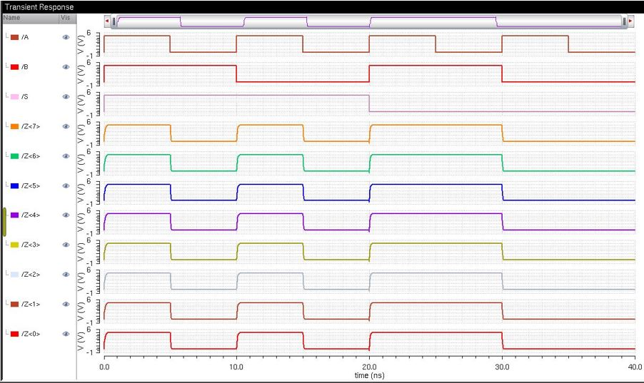
Below
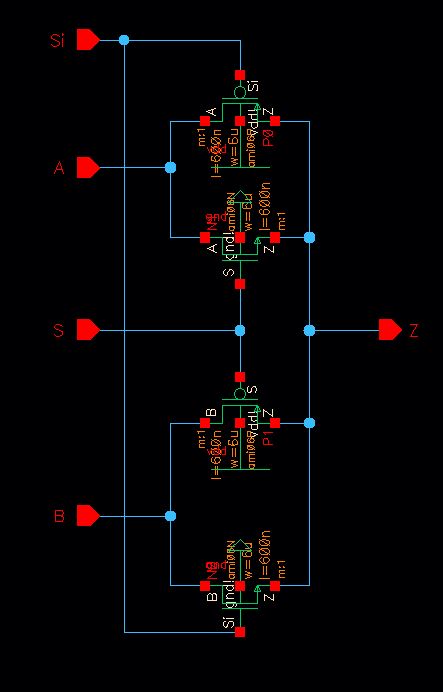
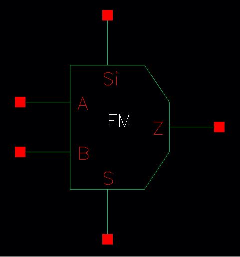
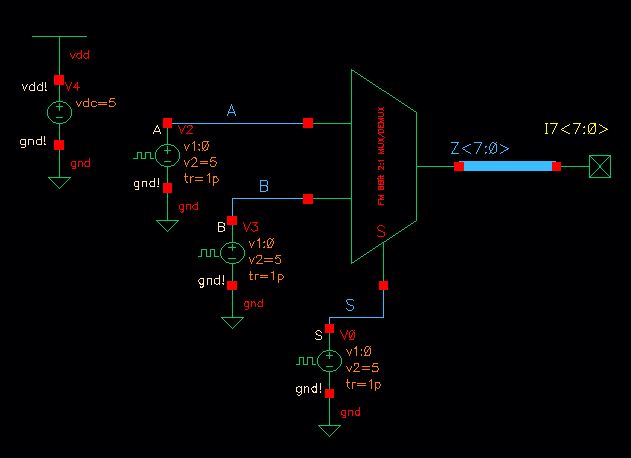
are the schematic, symbol, and simulations for the 2-1 DEMUX/MUX
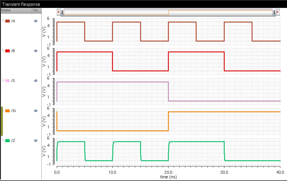
The
plot below shows that the 2-1 MUX is a 2 to 1 switch being selected by S. So,
when S is high and Si (S inverted) is low, the PMOS and NMOS connected to input
A are on. Thus, allowing the data on A to pass to output Z. When S is low, and
Si is high, the PMOS and NMOS connected to input B are on. This time the data
on B is passed to the output Z.
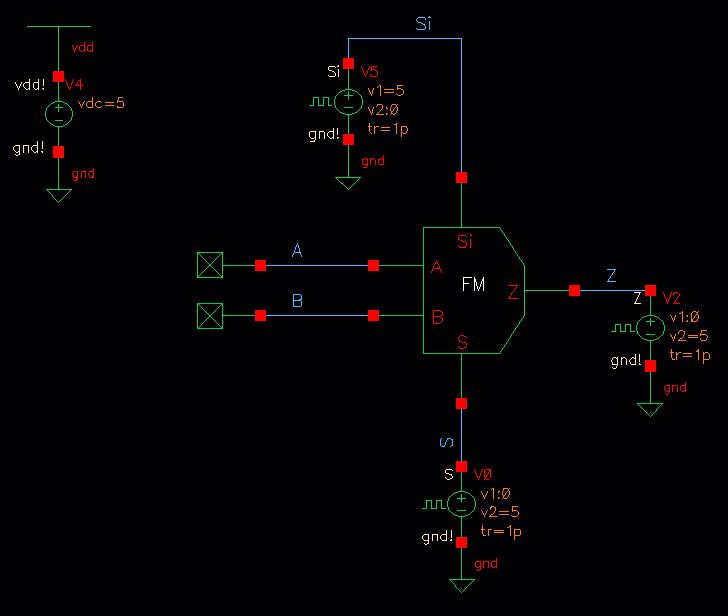
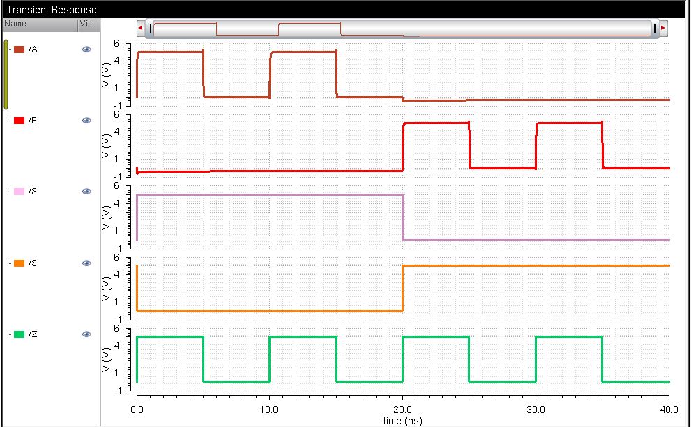
The
plot below shows how this circuit can be use as a 2-1 DEMUX. If the input is
connected to Z, then depending on selector S, the data from Z will be fed to A
or B. If S is high and Si is low, the input from Z will be fed to A. And if S
is low and Si is high, then the data will be fed to B.
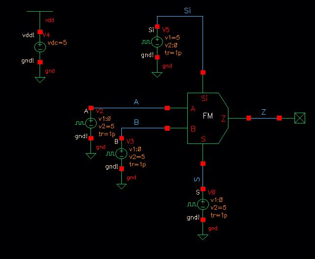
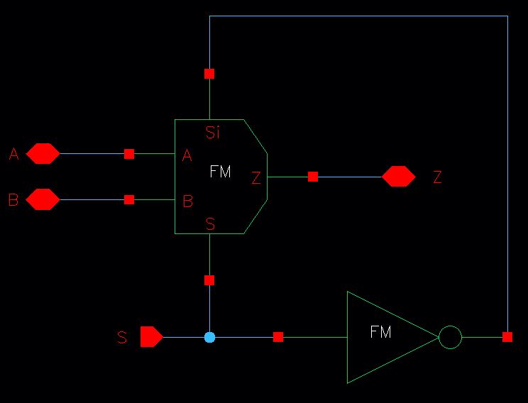
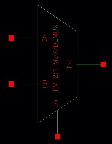
2-1
DEMUX/MUX schematic and symbol using an inverter to have one input selector
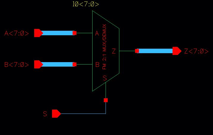
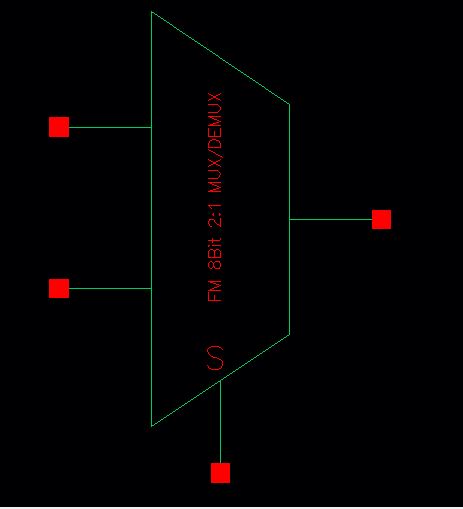
8-bit
2-1 DEMUX/MUX schematic, symbol, and simulation
Below
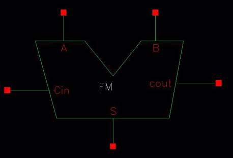
is the schematic and symbol for the CMOS AOI implementation of a full adder.
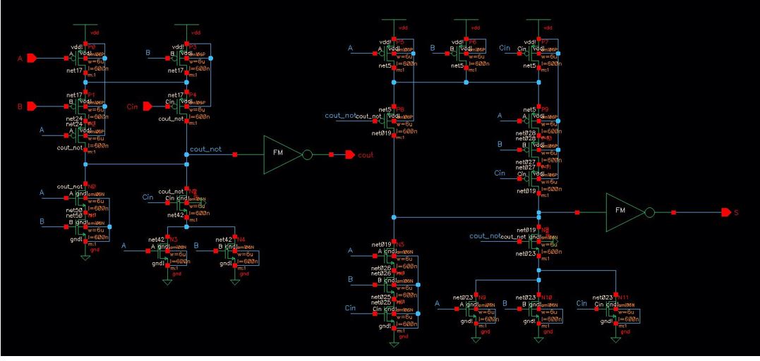
Below
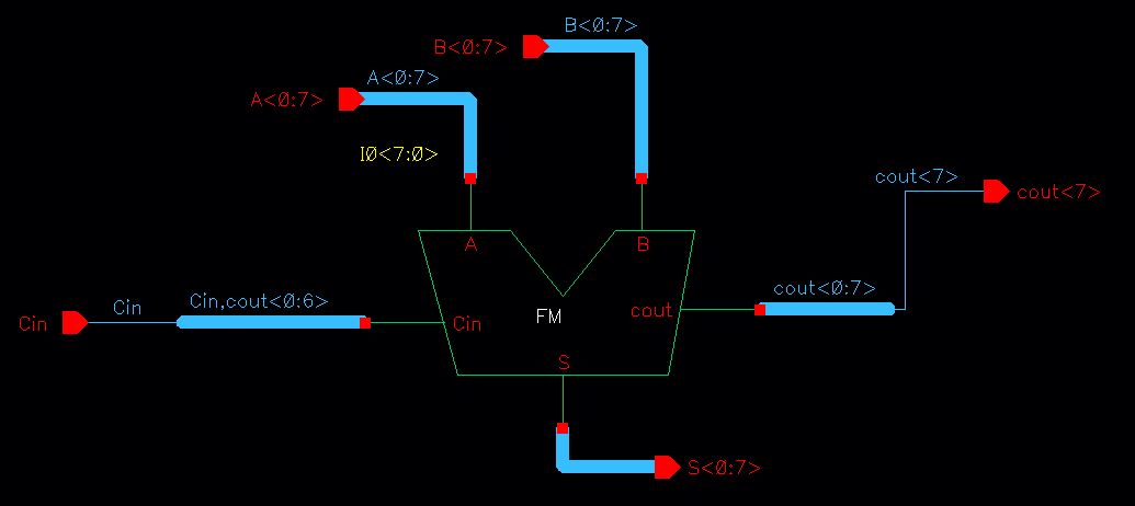
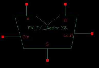
is the 8-bit Full-Adder schematic and symbol
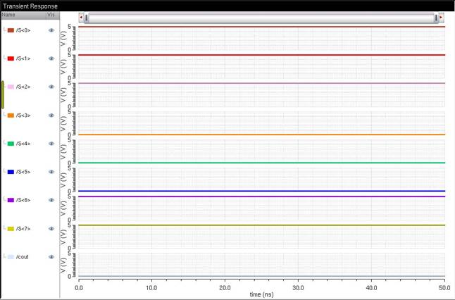
Below
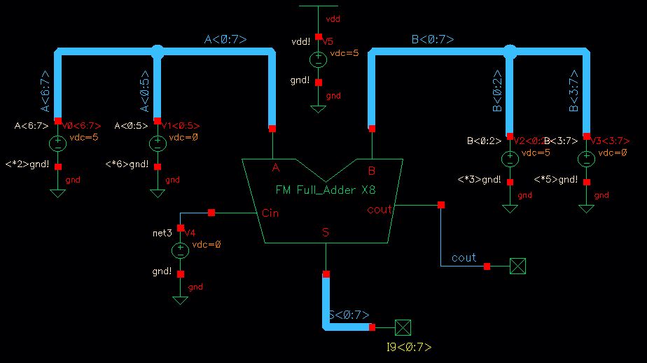
is the simulation for the 8-bit Adder. The plot below shows the outcome after
adding two bytes A and B, with digits 11000000 and 00000111 respectively, with
result 11000111.
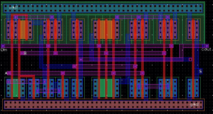
Below
are the layout and extracted view for the AOI Full Adder
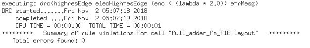
Below
are the DRC and LVS for the Adder above
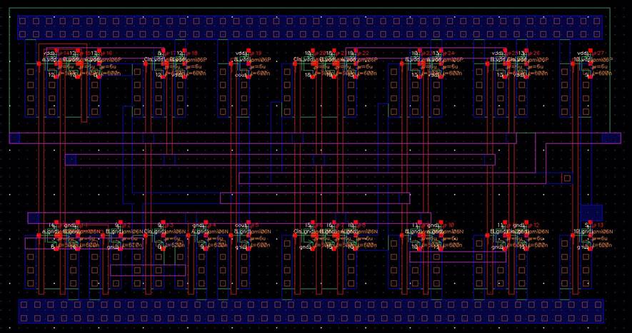
Below
are the Layout and extracted view for the 8-bit AOI Full Adder


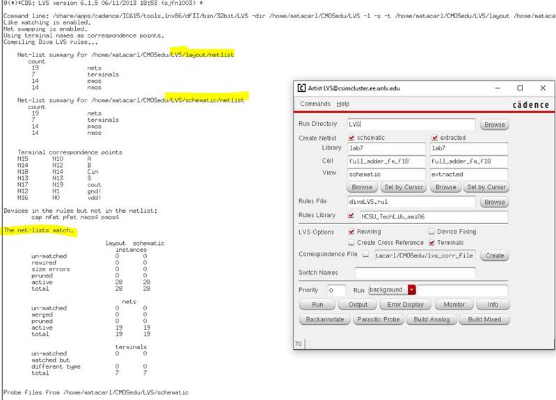
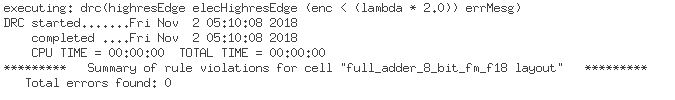
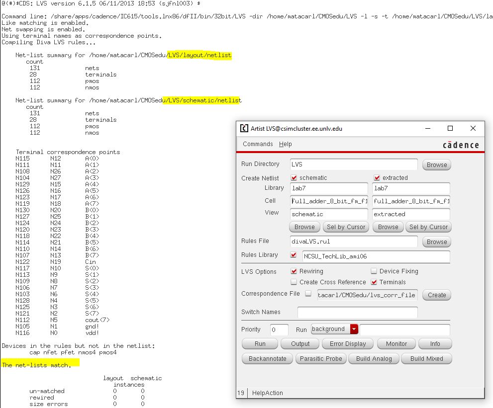
Below
are the DRC and LVS for the 8-bit Adder above
Layout, schematic, and simulation files can be found here lab7_fmc
Return to student lab reports
Return to labs