Lab 6 - EE 421L Design, Layout, and simulate of a CMOS NAND gate, XOR gate, and Full-Adder
Francisco Mata Carlos
email: matacarl@unlv.nevada.edu
10/24/18
Pre-lab :
- The files from the lab and the course were backed-up on google drive
- Followed and watched Tutorial 4 seen here.
- And read through the lab in its entirely before starting the actual lab
Lab
description:
The
goal of this lab is to design, layout and simulate a 2-input NAND gate
and a 2-input XOR gate using 6u/0.6u MOSFETs (NMOS and PMOS). Also,
design a Full Adder using the NAND gate and XOR gate.
Below are the 2-input NAND gate schematic, symbol, extracted and layout
Below are the DRC and LVS results for the NAND gate
Below are the 2-input XOR gate schematic, symbol, extracted and layout
Below are the DRC and LVS results for the XOR gate
Below are the schematic and simulation for the inverter, NAND, and XOR
Truth table for NAND and XOR gate

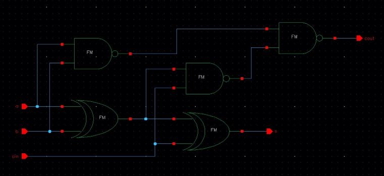
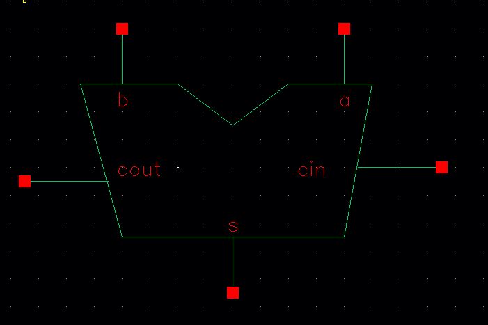
Below are the Full Adder schematic, symbol, extracted and layout
| http://cmosedu.com/jbaker/courses/ee421L/f18/students/matacarl/Lab%206/full_adder_LVS.JPG |
Below are the DRC and LVS results for the Full Adder
Full Adder schematic and simulation results
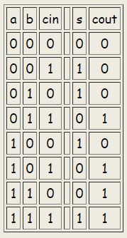
Full Adder truth table

Layout, schematic, and simulation files can be found here lab6_fmc
Return to student lab reports
Return to labs