Lab 4 - IV characterisctics and layout of NMOS and PMOS Devices - EE 421L 

Francisco Mata Carlos

email: matacarl@unlv.nevada.edu

 9/24/18

Pre-lab:

Backed-up all files from the lab and course on google drive. And read through lab 4.
Finished watching Tutorial 2

Lab description:

This lab focus is to run several NMOS and PMOS simulations, and to layout those devices with probe pads connected to their terminals.

Part 1) 
Generate 4 schematics and simulations (see the examples in the Ch6_IC61 library but note that for the PMOS body should be at vdd! instead of gnd!)

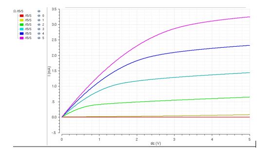
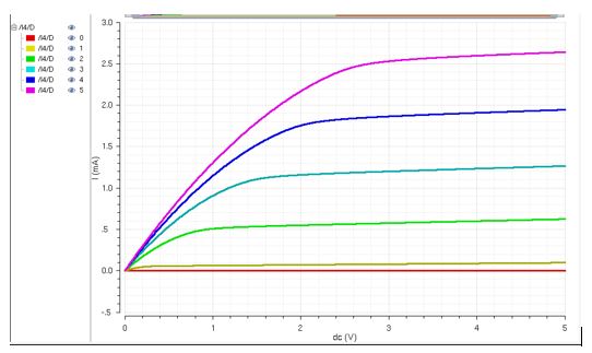
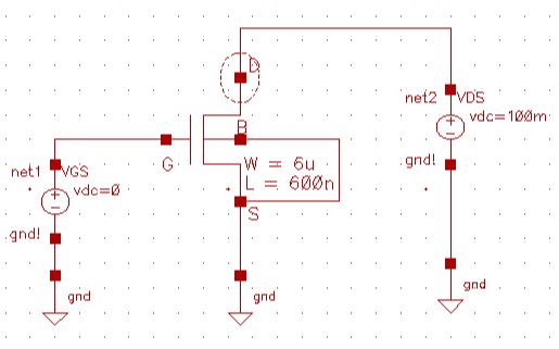
a)    a) A schematic for simulating ID v. VDS of an NMOS device for VGS varying from 0 to 5 V in 1 V steps while VDS varies from 0 to 5 V in 1 mV steps. Use a 6u/600n width-to-length ratio
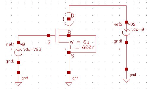
http://cmosedu.com/jbaker/courses/ee421L/f18/students/matacarl/Lab%204/pic2.JPG http://cmosedu.com/jbaker/courses/ee421L/f18/students/matacarl/Lab%204/pic1.JPG

a)    
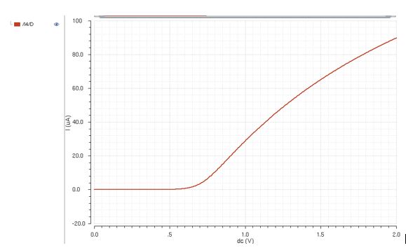
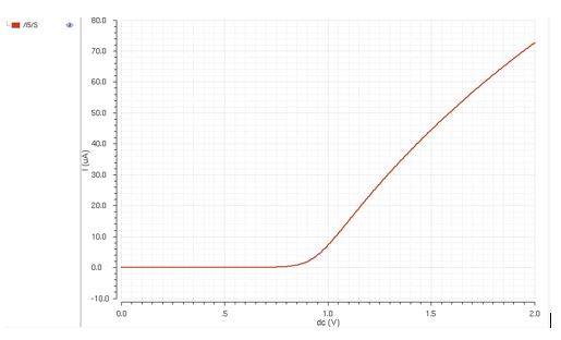
b) A schematic for simulating ID v. VGS of an NMOS device for VDS = 100 mV where VGS varies from 0 to 2 V in 1 mV steps. Again, use a 6u/600n width-to-length ratio. 

http://cmosedu.com/jbaker/courses/ee421L/f18/students/matacarl/Lab%204/pic5.JPG http://cmosedu.com/jbaker/courses/ee421L/f18/students/matacarl/Lab%204/pic4.JPG

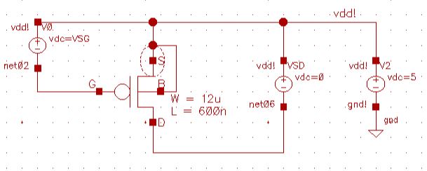
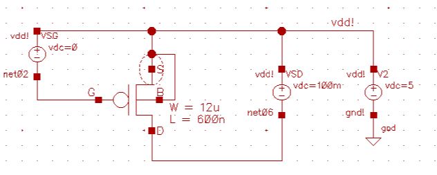
a)    c) A schematic for simulating ID v. VSD (note VSD not VDS) of a PMOS device for VSG (not VGS) varying from 0 to 5 V in 1 V steps while VSD varies from 0 to 5 V in 1 mV steps. Use a 12u/600n width-to-length ratio.

      http://cmosedu.com/jbaker/courses/ee421L/f18/students/matacarl/Lab%204/pic3.JPG http://cmosedu.com/jbaker/courses/ee421L/f18/students/matacarl/Lab%204/pic6.JPG

a)    d) A schematic for simulating ID v. VSG of a PMOS device for VSD = 100 mV where VSG varies from 0 to 2 V in 1 mV steps. Again, use a 12u/600n width-to-length ratio.

http://cmosedu.com/jbaker/courses/ee421L/f18/students/matacarl/Lab%204/pic7.JPG   http://cmosedu.com/jbaker/courses/ee421L/f18/students/matacarl/Lab%204/pic8.JPG


Part 2)
Lay out a 6u/0.6u NMOS device and a 12u/0.6u PMOS device, and connect all 4 MOSFET terminals to probe pads

According to MOSIS design rules the minimum probe pad is 20um. The pad in this this case was chosen to be a little bigger, with 33.6um per side using Metal3 layer and 21.6um per side for the Glass layer.

http://cmosedu.com/jbaker/courses/ee421L/f18/students/matacarl/Lab%204/probe_pad_min_size.JPG  
http://cmosedu.com/jbaker/courses/ee421L/f18/students/matacarl/Lab%204/probe_pad.JPG  http://cmosedu.com/jbaker/courses/ee421L/f18/students/matacarl/Lab%204/probe_pad_schematic.JPG

Lay out a 6u/0.6u NMOS device and connect all 4 MOSFET terminals to probe pads (which can be considerably smaller than bond pads and directly adjacent to the MOSFET (so the layout is relative small).3

 
http://cmosedu.com/jbaker/courses/ee421L/f18/students/matacarl/Lab%204/pic10.JPG
     http://cmosedu.com/jbaker/courses/ee421L/f18/students/matacarl/Lab%204/pic11.JPG
 
http://cmosedu.com/jbaker/courses/ee421L/f18/students/matacarl/Lab%204/pic9.JPG  http://cmosedu.com/jbaker/courses/ee421L/f18/students/matacarl/Lab%204/pic13.JPG

http://cmosedu.com/jbaker/courses/ee421L/f18/students/matacarl/Lab%204/pic12.JPG

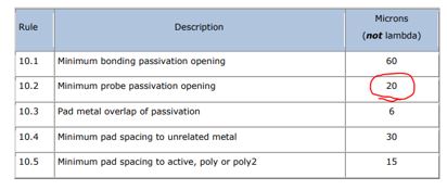
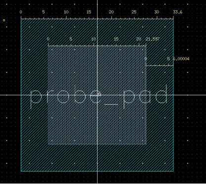
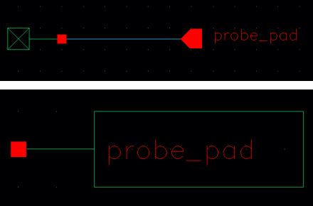
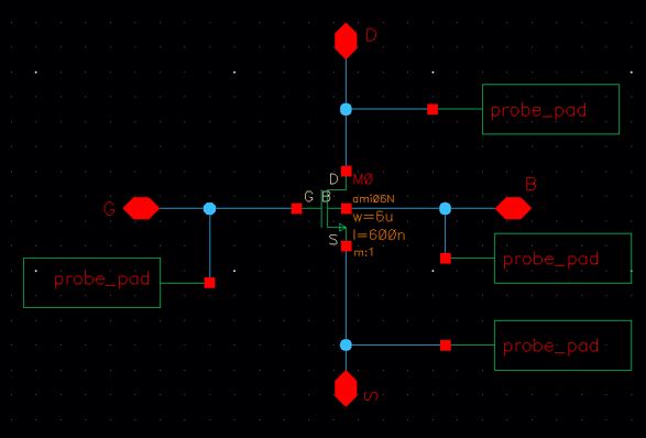
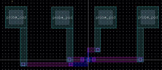
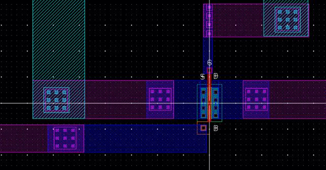
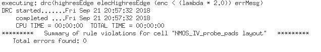
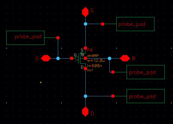
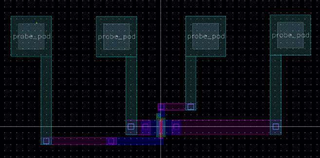
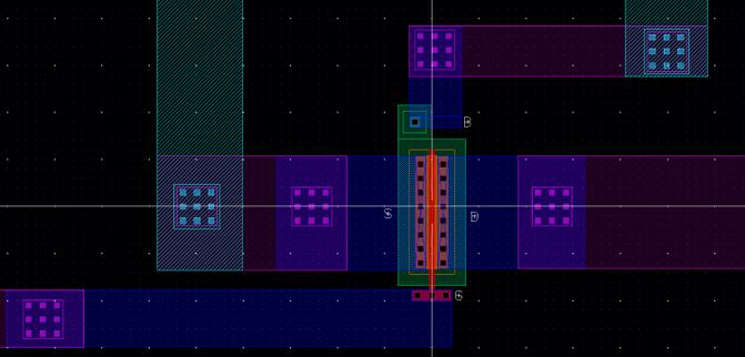
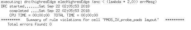
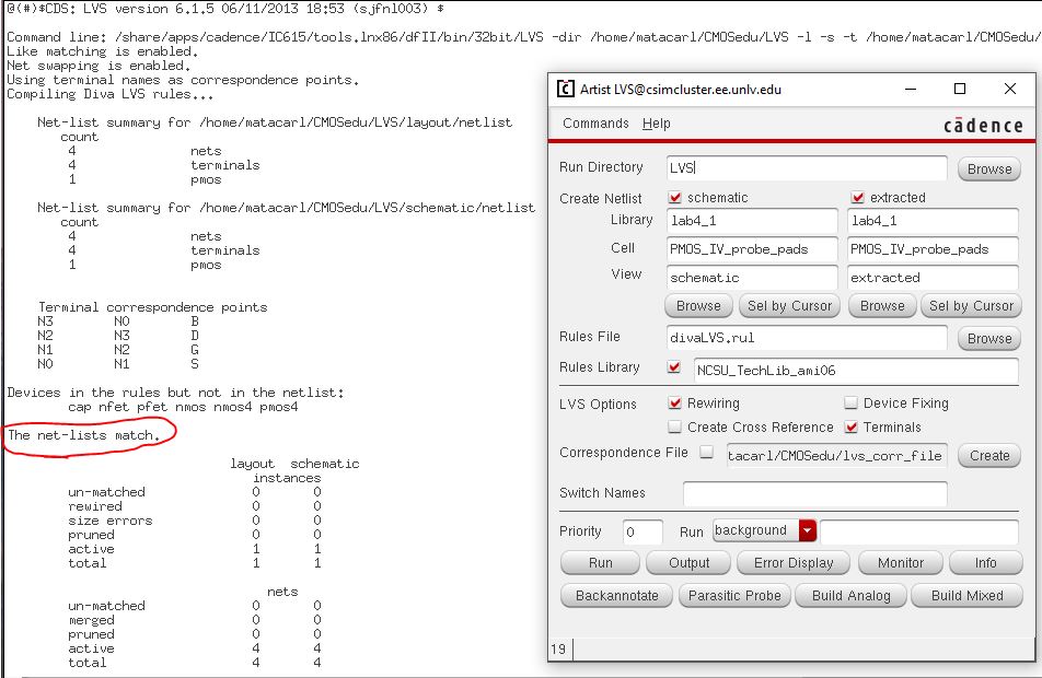
Lay out a 12u/0.6u PMOS device and connect all 4 MOSFET terminals to probe pads.


http://cmosedu.com/jbaker/courses/ee421L/f18/students/matacarl/Lab%204/PMOS_1.JPG  http://cmosedu.com/jbaker/courses/ee421L/f18/students/matacarl/Lab%204/PMOS3.JPG

http://cmosedu.com/jbaker/courses/ee421L/f18/students/matacarl/Lab%204/PMOS2.JPG  http://cmosedu.com/jbaker/courses/ee421L/f18/students/matacarl/Lab%204/PMOS4.JPG

http://cmosedu.com/jbaker/courses/ee421L/f18/students/matacarl/Lab%204/PMOS5.JPG


Return to student lab reports

Return to labs