Lab 3 - EE 421L
Francisco Mata Carlos
email: matacarl@unlv.nevada.edu
9/19/18
Pre-lab:
Backed up all the previous work from lab
and the course by uploading them to google drive.
Finished Tutorial 1.
Lab
description:
Design a 10k resistor using n-well layer as
shown in Tutorial 1. Use that design to layout a R-2R DAC by placing the resistors on
top of each other creating a stacked.
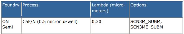
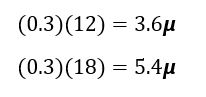
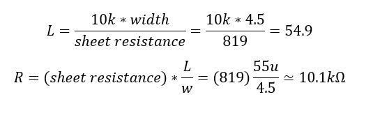
Referring to the process information from
MOSIS we can see that the minimum width is 3.6u and minimum well space is 5.4u.
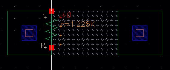
The sheet resistance was found by using the minimum values
for length (5.4u) and width (3.6u) to make a test resistor and extracted it to
obtain a more precise result. The resistance came to be 1.228kΩ.

For the 10K
resistor the formulas below were used, and a value of 4.5u was used as the width.
So, the length was solved first and then plugged into the second equation to calculate and estimate the value of the resistor.
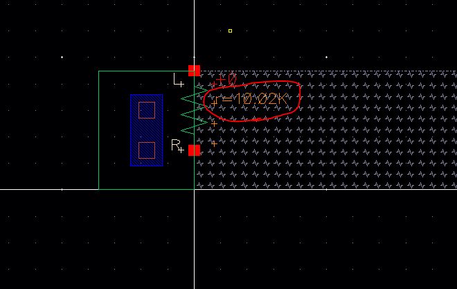
Below is the value of the resistor from the extracted view
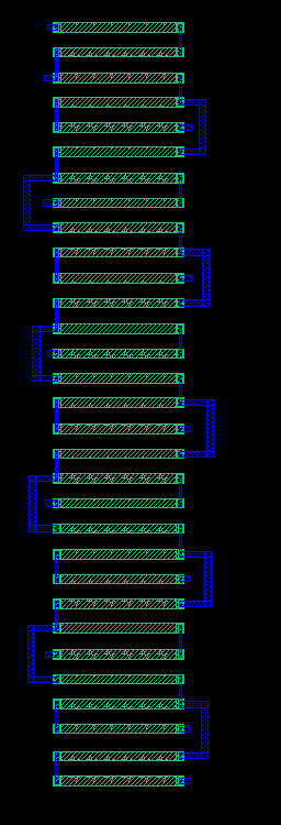
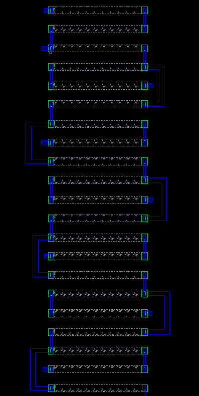
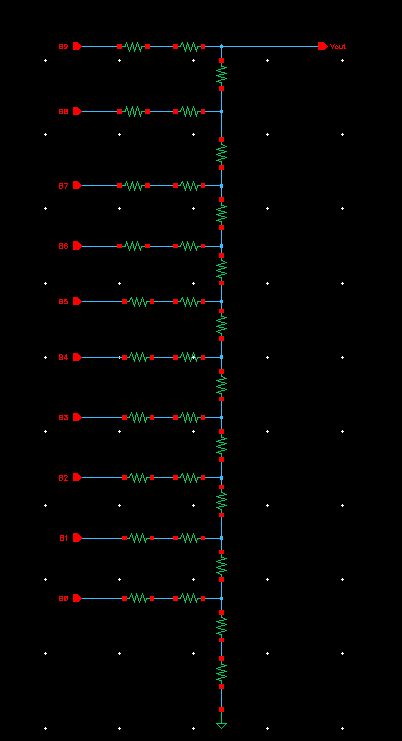
Below is a snap
shot of the layout, extracted view and schematic of the DAC using R-2R topology
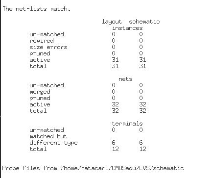
After
running Layout versus Schematic (LVS) the output result, below, shows that the
net-list matches for the layout and the schematic.
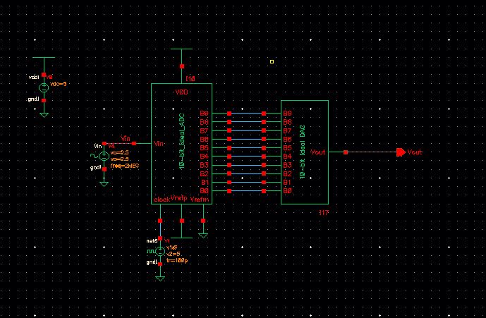
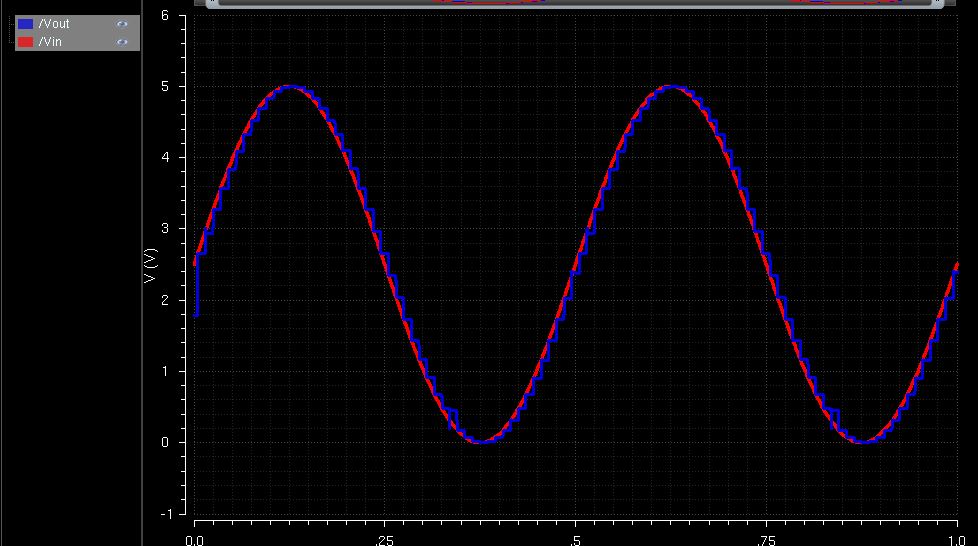
The
plot below shows the simulation after the extracted file was simulated,
which matches the output simulation that was shown on lab 2. This
simulation is running the ADC_DAC with no load
Layout, schematic, and simulation files can be downloaded here
Return to student lab reports
Return to labs