Lab 1 - EE 421L
Pre-lab:
A CMOSedu account
was requested using my UNLV email address from Dr. Baker, rjacobbaker@gmail.com.
Also, the material
seen here about
editing webpages was reviewed, prior to the first lab.
Lab Description:
This lab’s focus
has two parts, one related to the first part of Tutorial 1, which introduces
how to install and use Cadence virtuoso. And the second is to discuss how the
lab files will be backup.
a) a) First part for lab 1
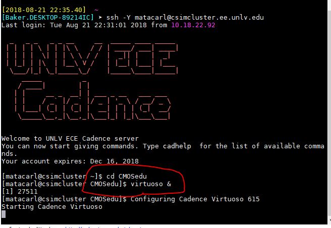
This consist of following Tutorial 1 from a set of tutorials found in Cadence webpage at CMOSedu.com. This tutorial explains how to properly set Cadence virtuoso on the computer in order to draw schematics and simulate them, and be able to make a layout, which is the design MOSIS uses in order to make a chip or die. This tutorial introduces the Cadence set-up for use with ON’s C5 process. First Xterm and NCSU Cadence Design Kit was downloaded to the desktop, then a set of instructions from the tutorial were followed. Once this was done correctly Cadence virtuoso could be open by using “virtuoso &”. Also, a directory call CMOSedu was created in which Cadence virtuoso can be open from.
Once
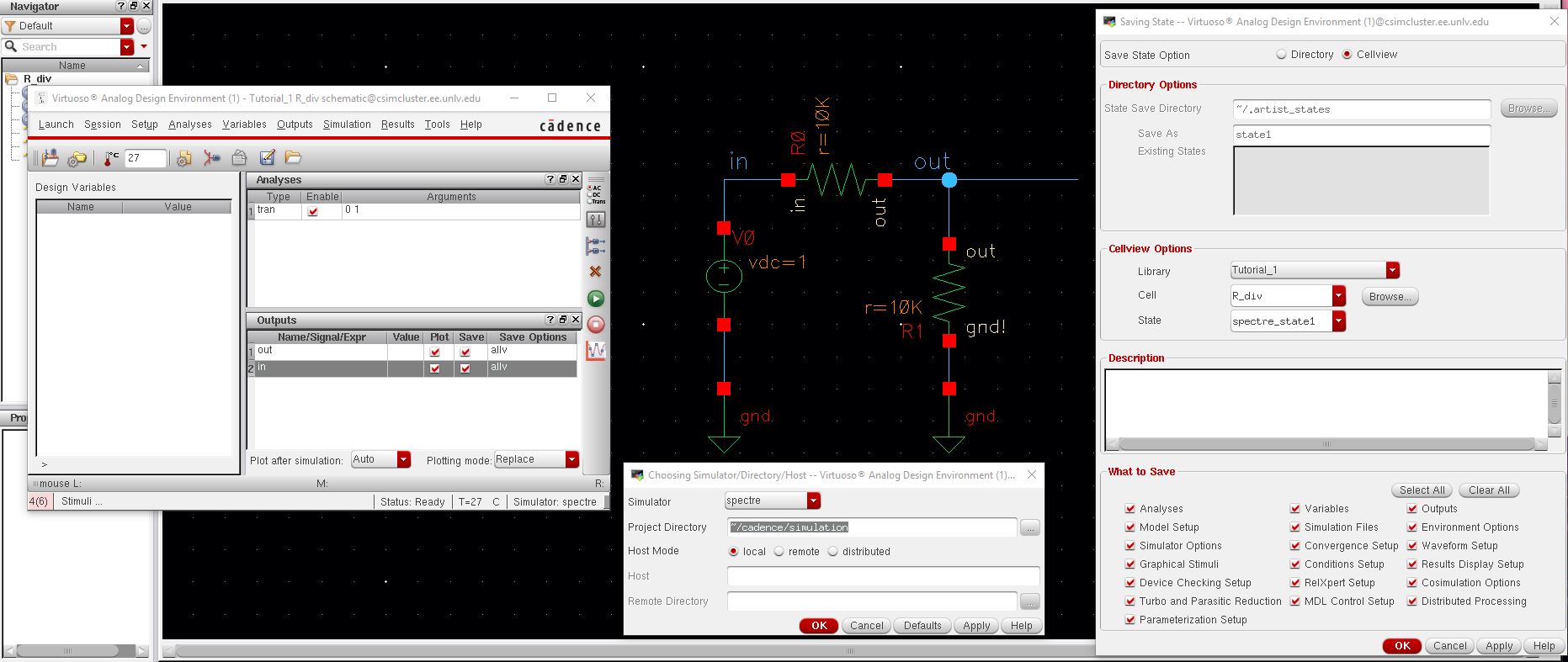
virtuoso was opened a library called “Tutorial_1” was created. In that library
a new cell with schematic view was also created, in which a voltage divided was
drawn. After the schematic was “check and save” without errors, then the Analog
Design Environment (ADE) was launched to simulate the schematic. Made sure the simulator
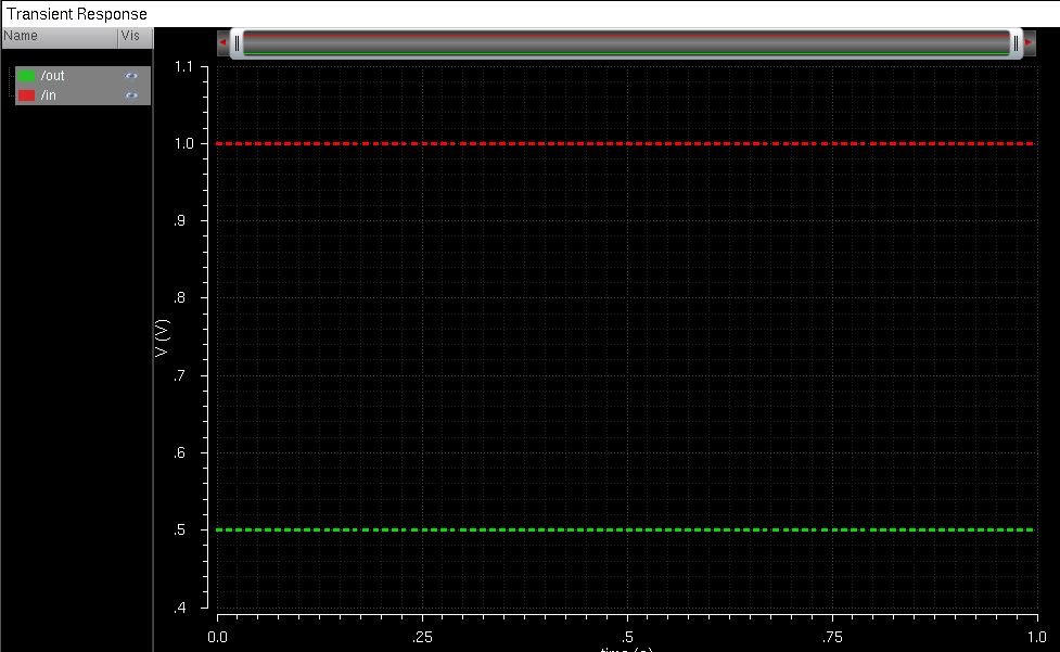
was spectre, and saved the state by clicking on cellview. Since the resistors
are equal in value or resistance, the output result is half of the input, as
shown below.
b) b) Second part for Lab 1
All my labs will be backed up by uploading them to google drive.
Return to student lab reports
Return to labs