Lab 7- EE 421L
Using buses and arrays in the design of word inverters, muxes, and high–speed adders
Authored
by Victor Martinez
martiv6@unlv.nevada.edu
November 3, 2018
Pre-lab work
- Back-up all of your work from the lab and the course.
- Go through Tutorial 5 seen here.
- Read through the entire lab before starting it.
Lab
description:
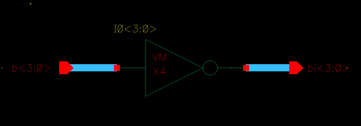
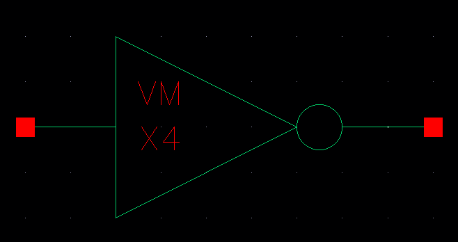
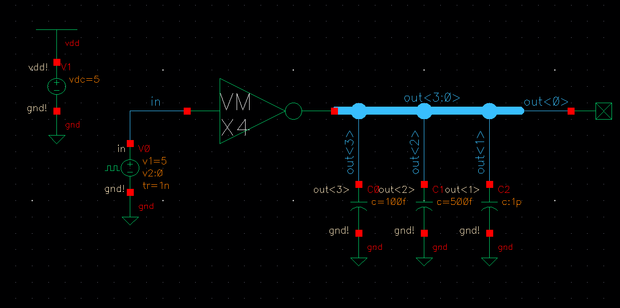
Schematic for 4 bit inverter
| Schematic | Symbol |
 |  |
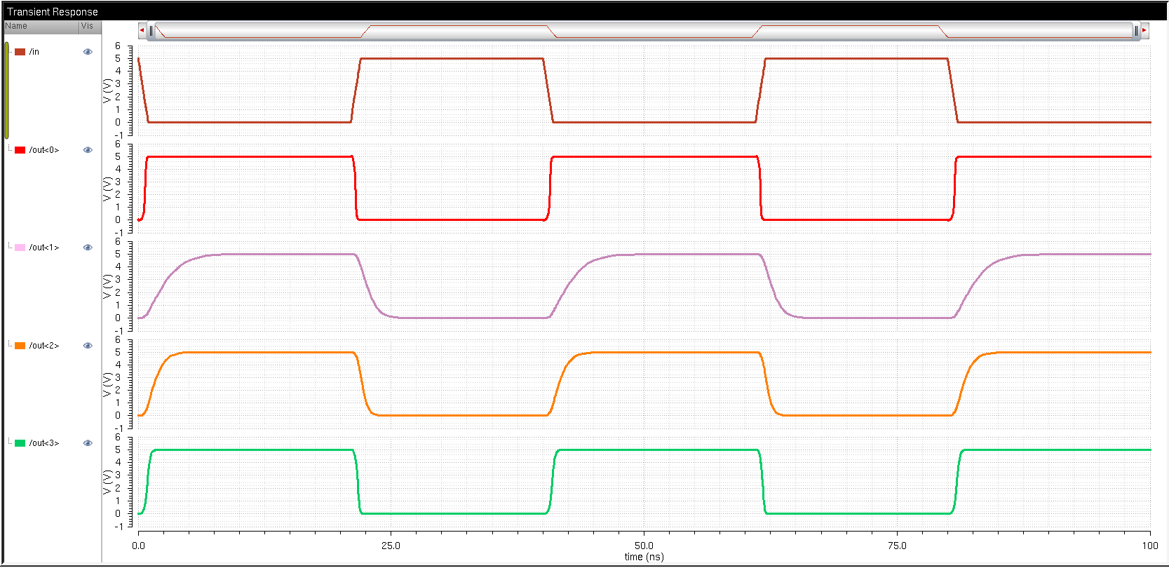
| Simulation of 4-bit Inverter | 4-bit inverter Plot |
 |  |
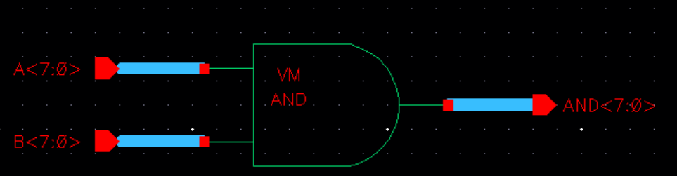
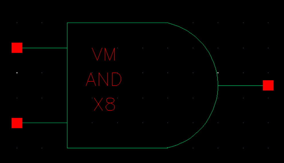
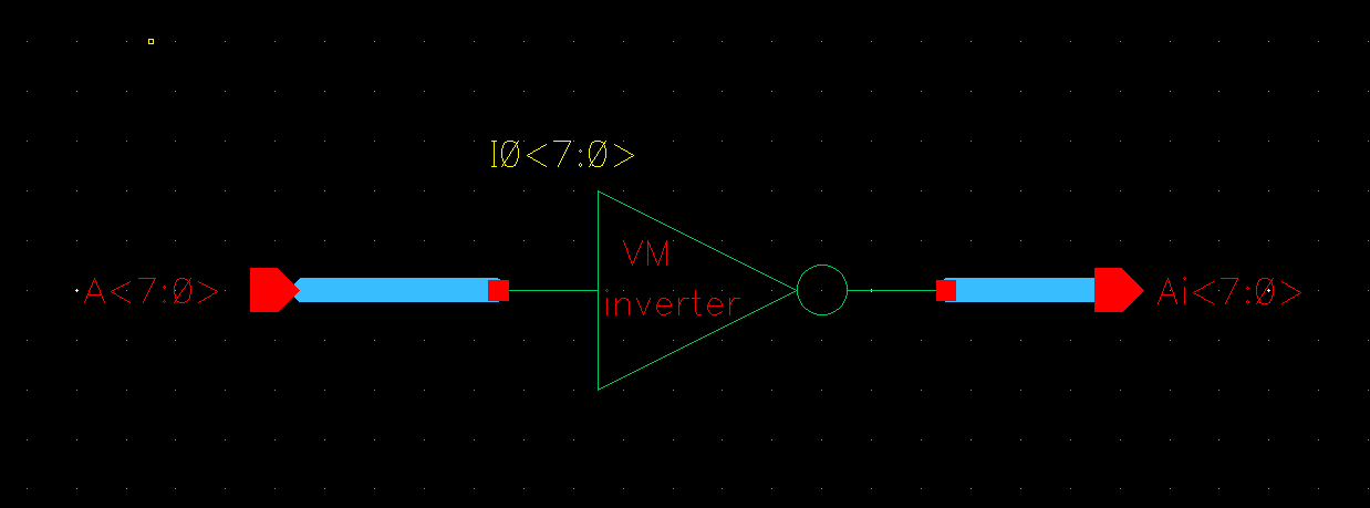
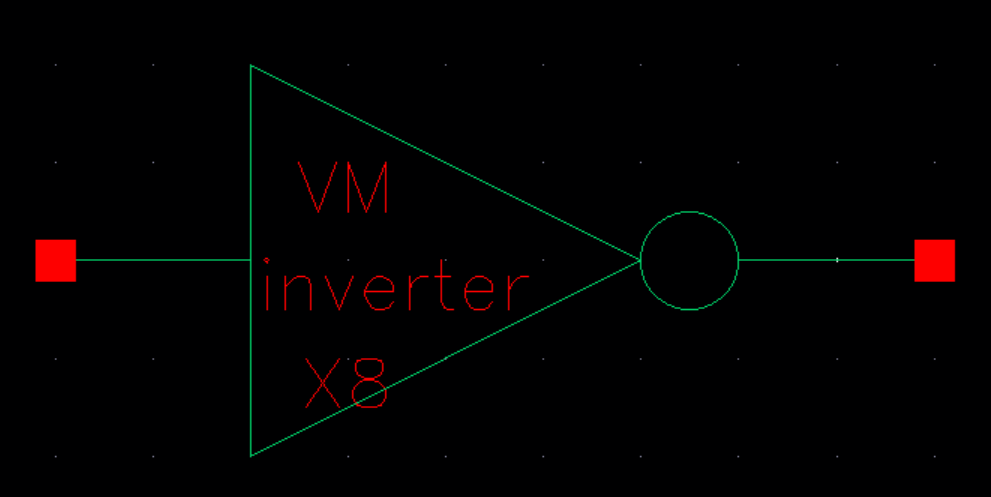
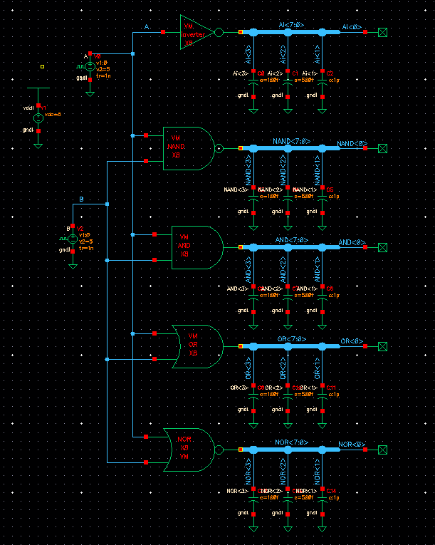
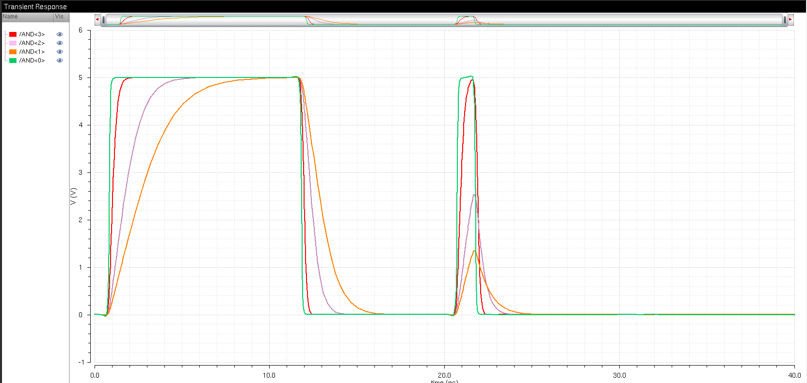
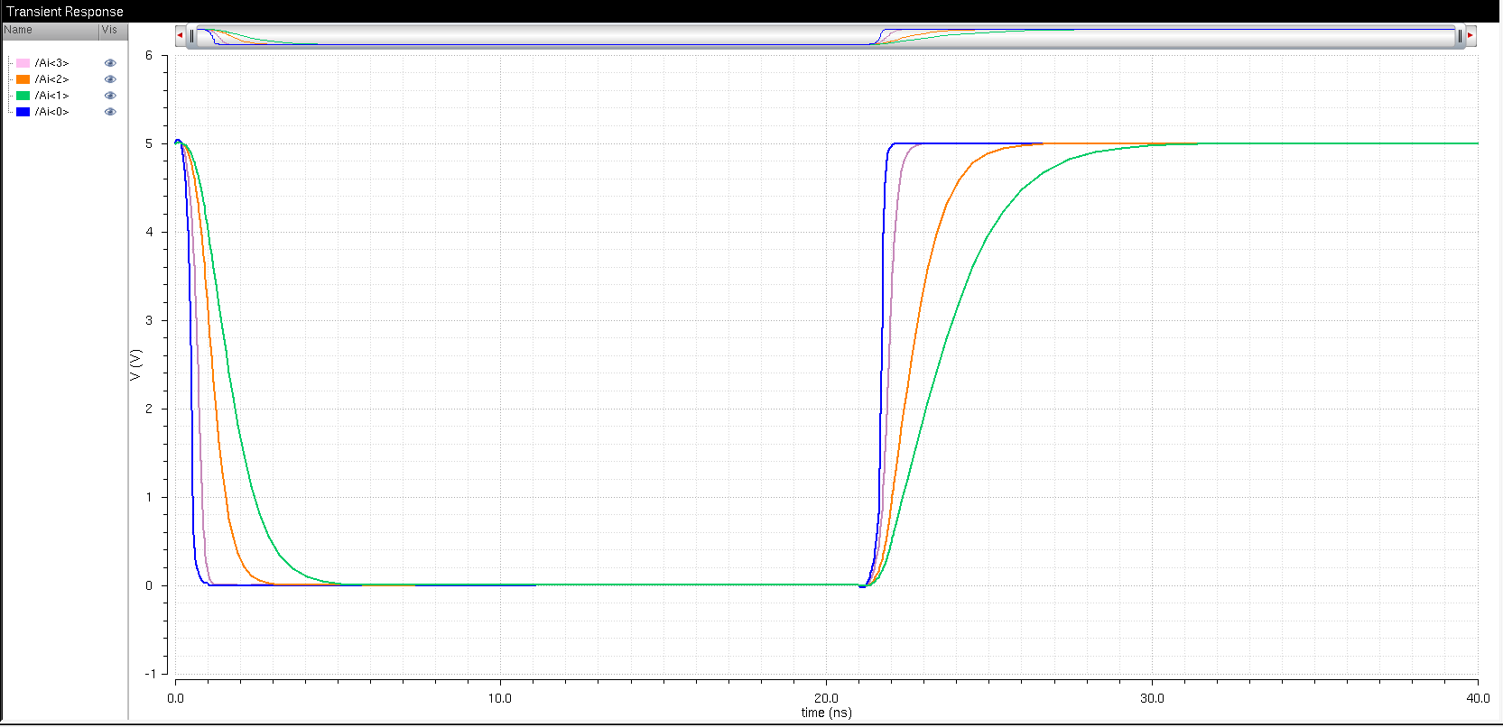
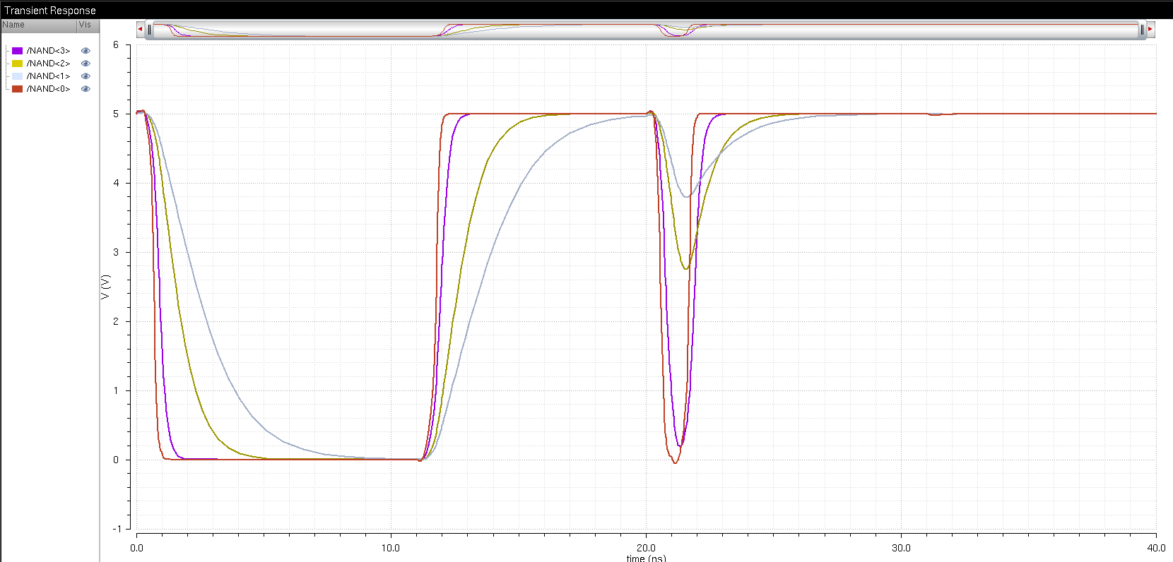
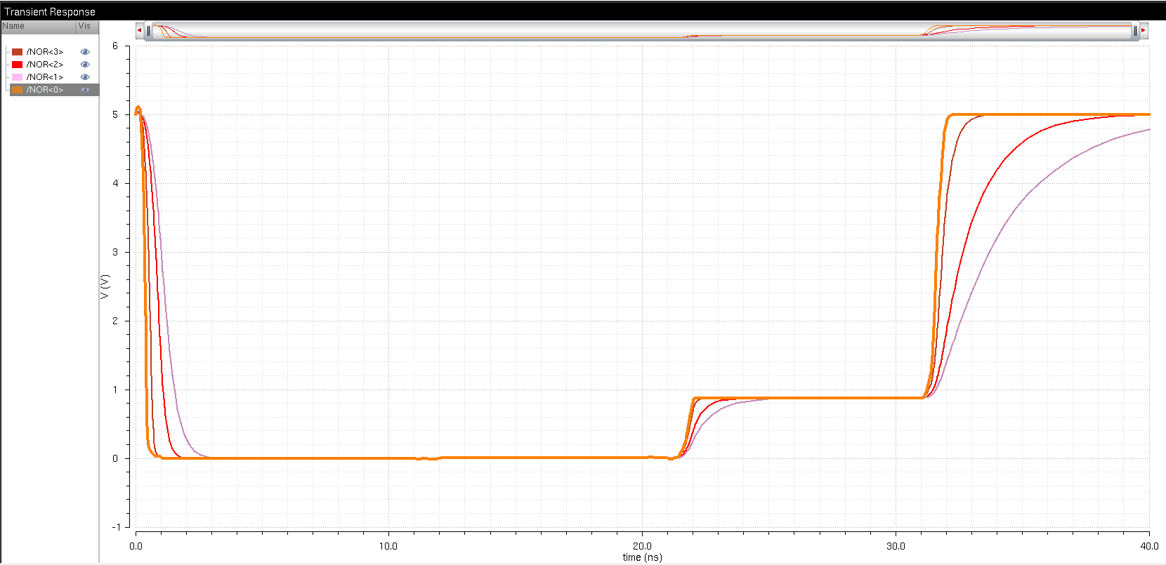
Schematics and Symbols for 8-bit: AND, inverter, NAND, NOR and OR
| AND Schematic | AND Symbol |
 |  |
| Inverter Schematic | Inverter Symbol |
 |  |
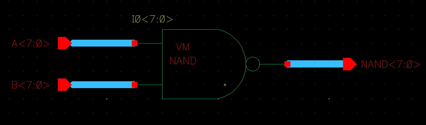
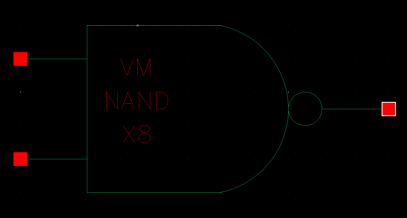
| NAND Schematic | NAND Symbol |
 |  |
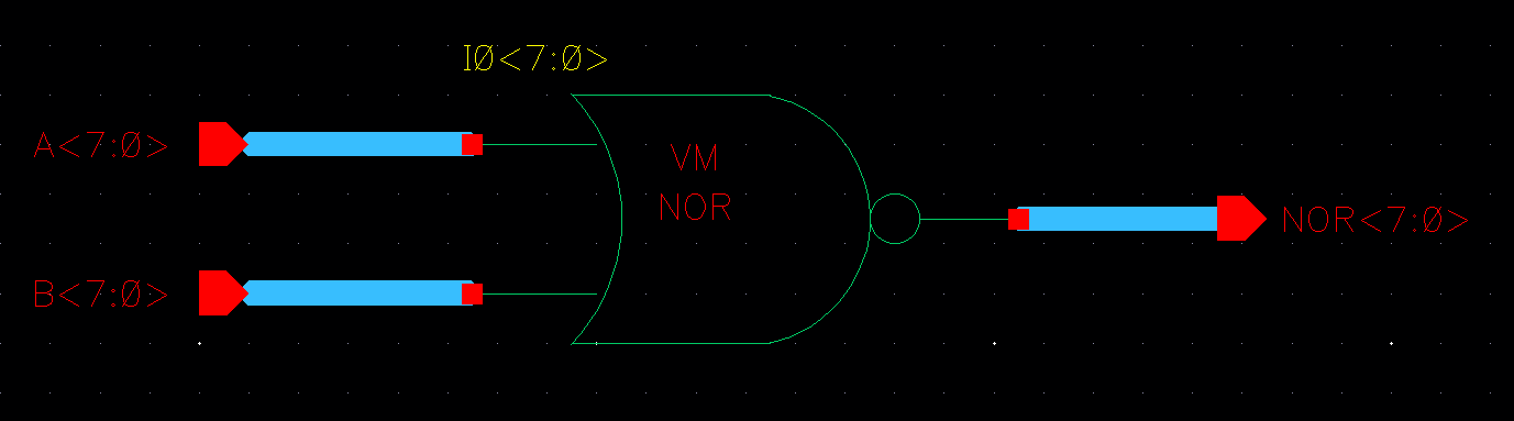
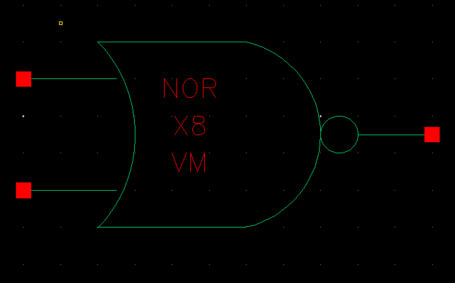
| NOR Schematic | NOR Symbol |
 |  |
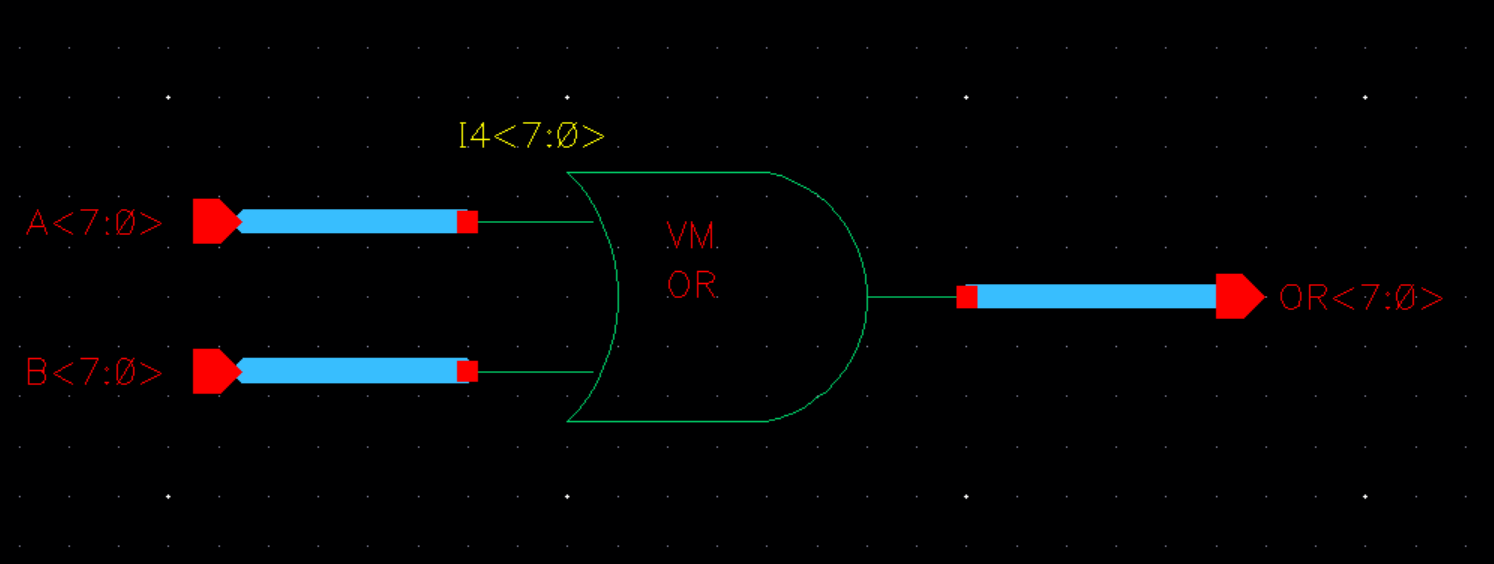
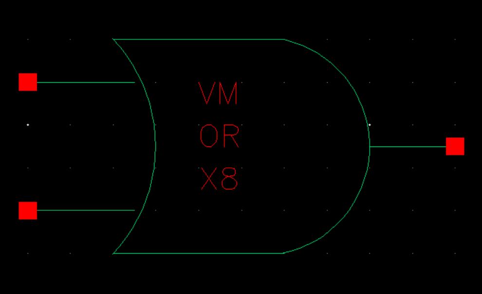
| OR Schematic | OR Symbol |
 |  |
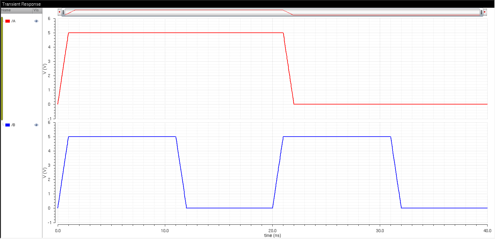
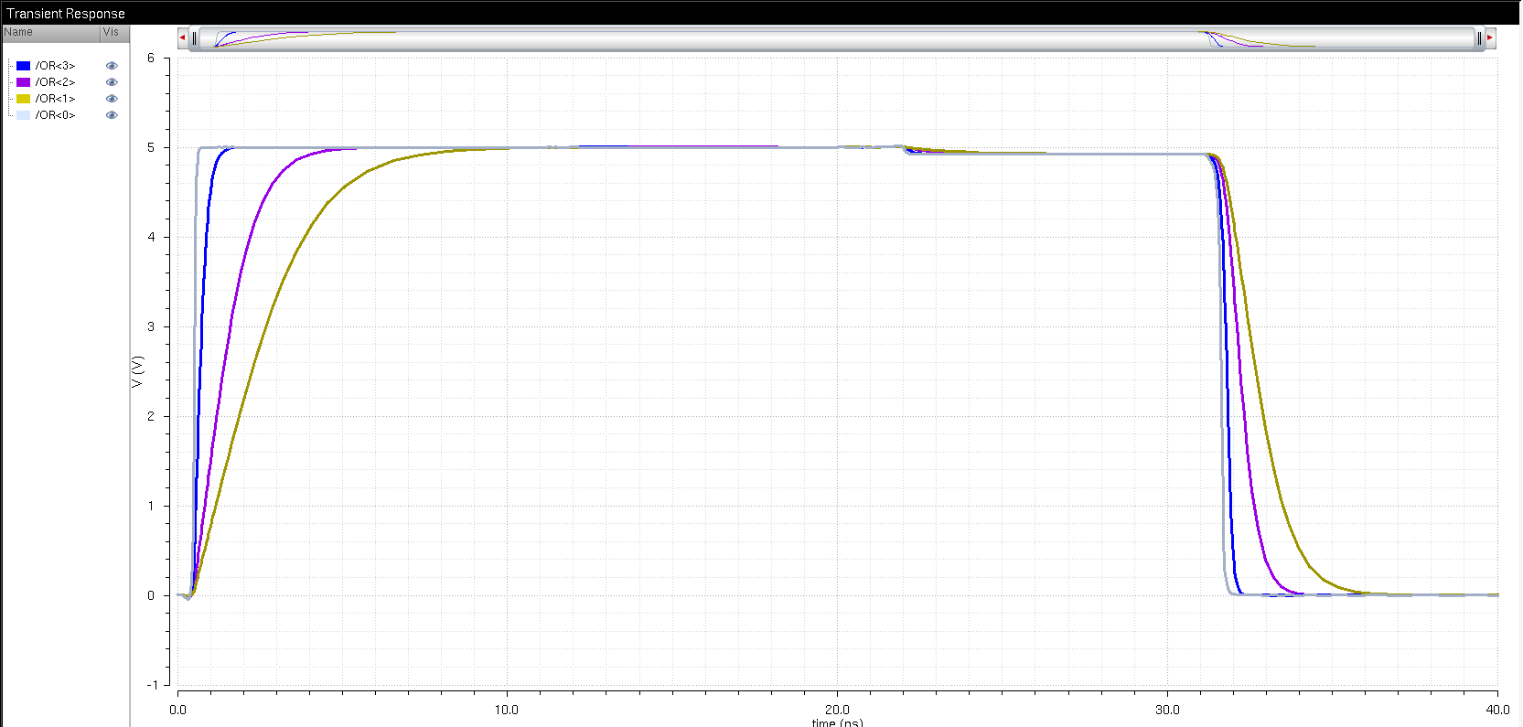
| 8-bit Gates Schematic | 8-bit Gates Plots |
 |  |
 |  |
 |  |
 | |
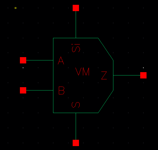
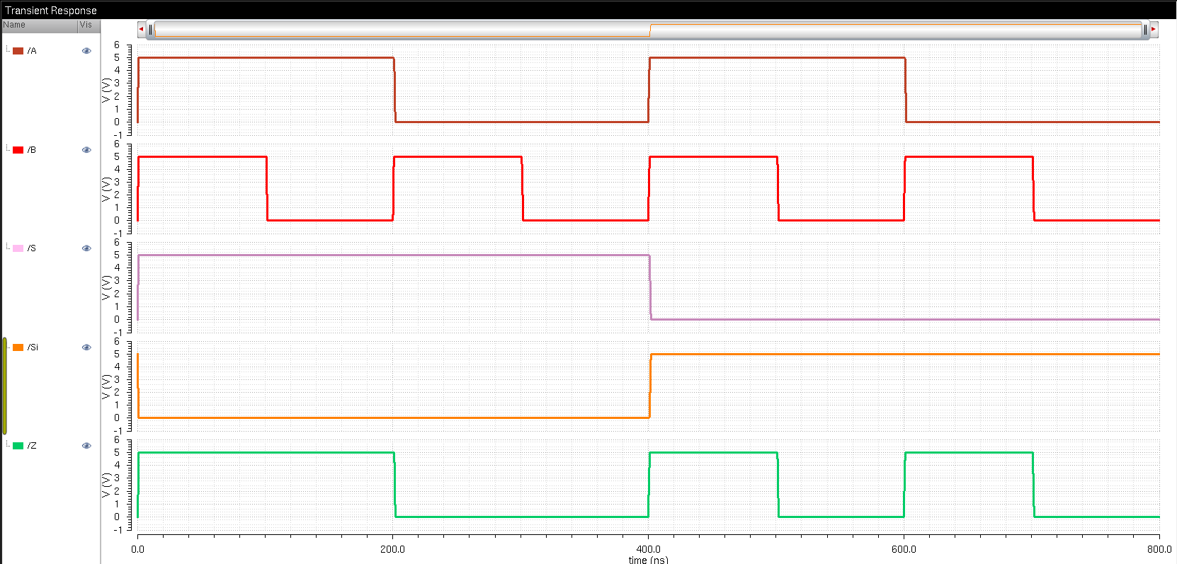
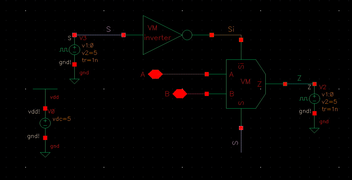
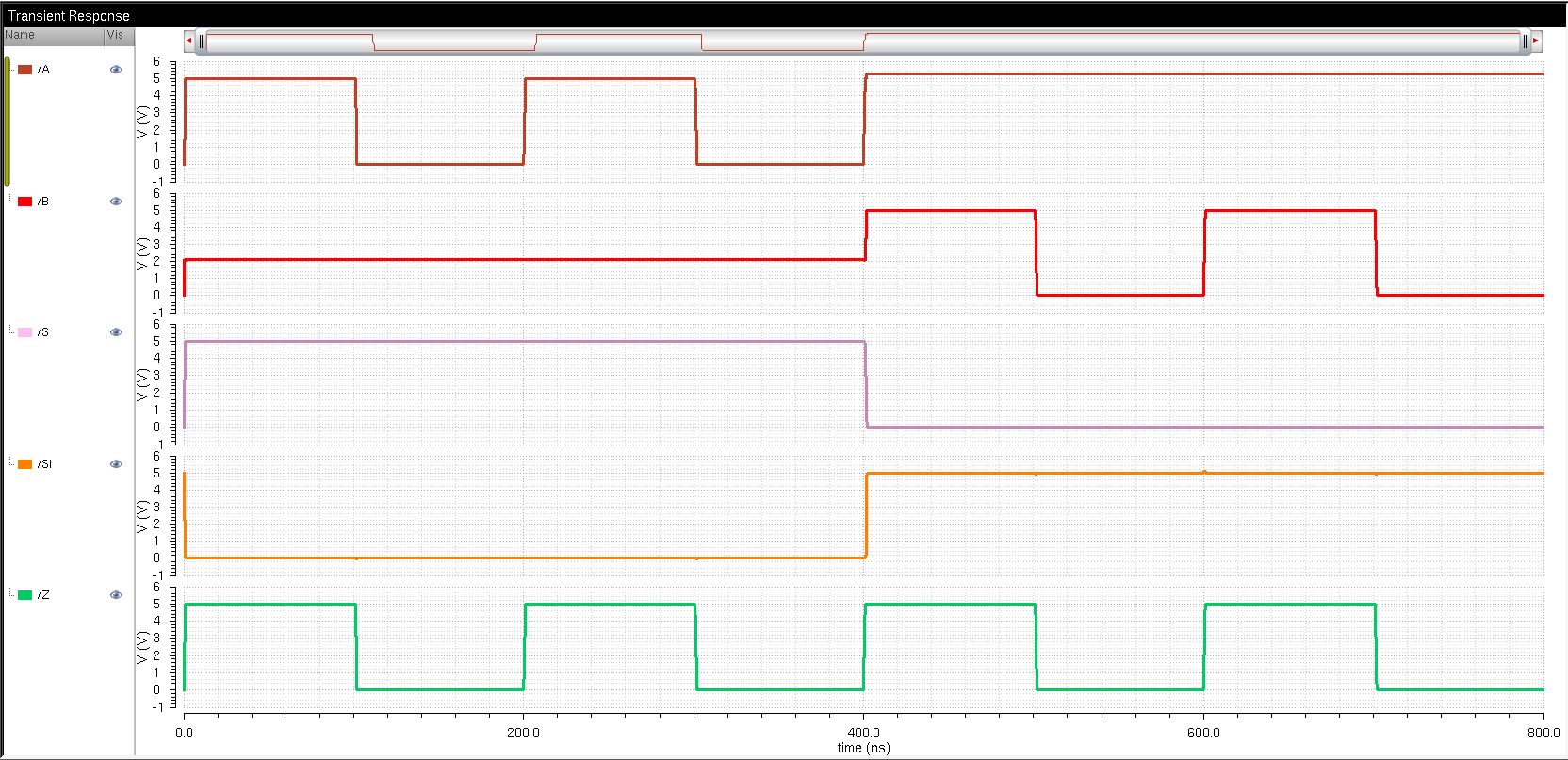
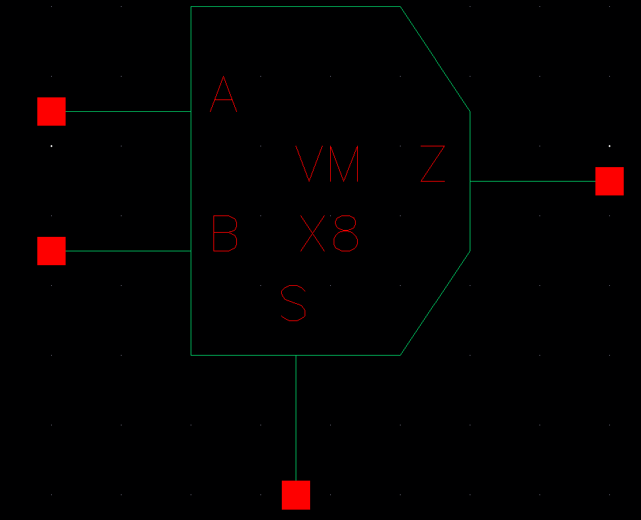
| 2-to-1 MUX Schematic | 2-to-1 Mux Symbol |
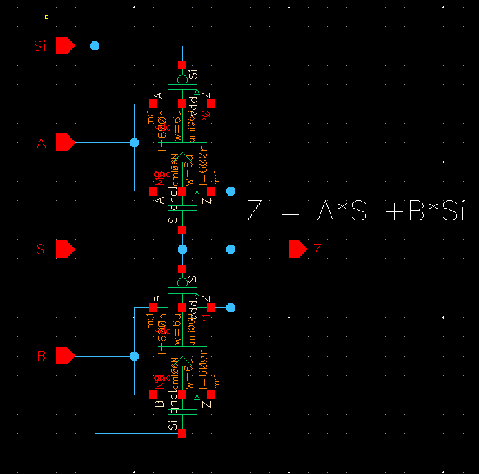 |  |
The
2-to-1 MUX output is defined as Z=A*S + B*Si and its inputs are A, B,
S, and Si. It allows one of the two inputs to be passed to Z when
selected by S. If the input at A is to be passed to Z then we set
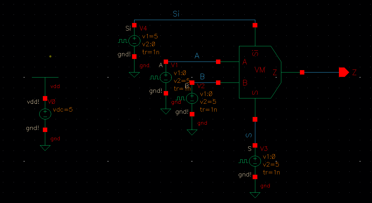
1 to S and 0 to Si.| 2-to-1 MUX Schematic | 2-to-1 MUX Schematic Plot |
 |  |
| 2-to-1 DEMUX Schematic | 2-to-1 DEMUX Plots |
 |  |
The
2-to-1 DEMUX output is defined as Z*S =A and Z*Si=B. It
allows one input to be passed to two outputs A and B when selected by
S. If the input to Z is to be passed to A then we set 1 to S and
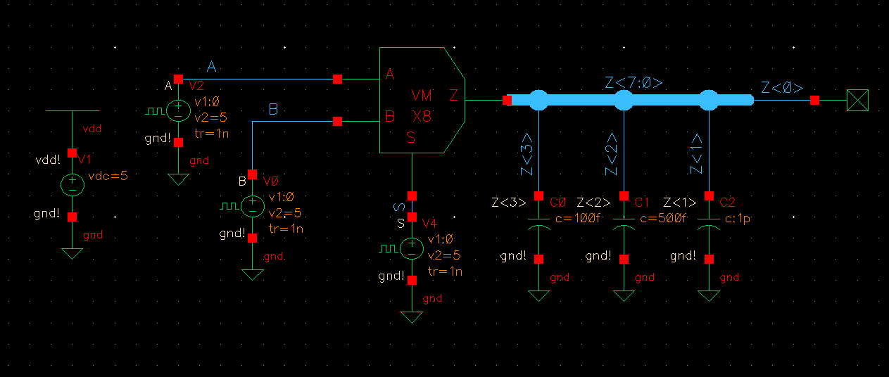
0 to Si.| 8-bit 2-to-1 DEMUX/MUX Schematic | 8-bit 2-to-1 DEMUX/MUX Symbol |
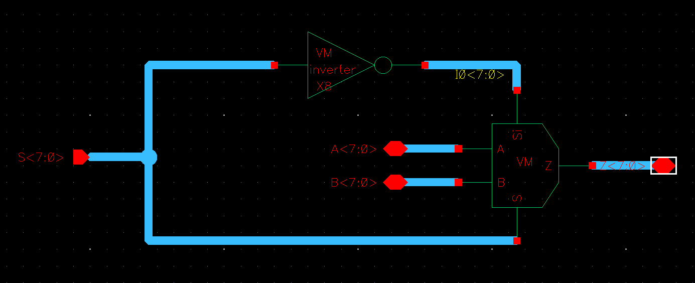 |  |
| Simulate 8-bit 2-to-1 DEMUX/MUX | 8-bit 2-to-1 DEMUX/MUX Plot |
 | 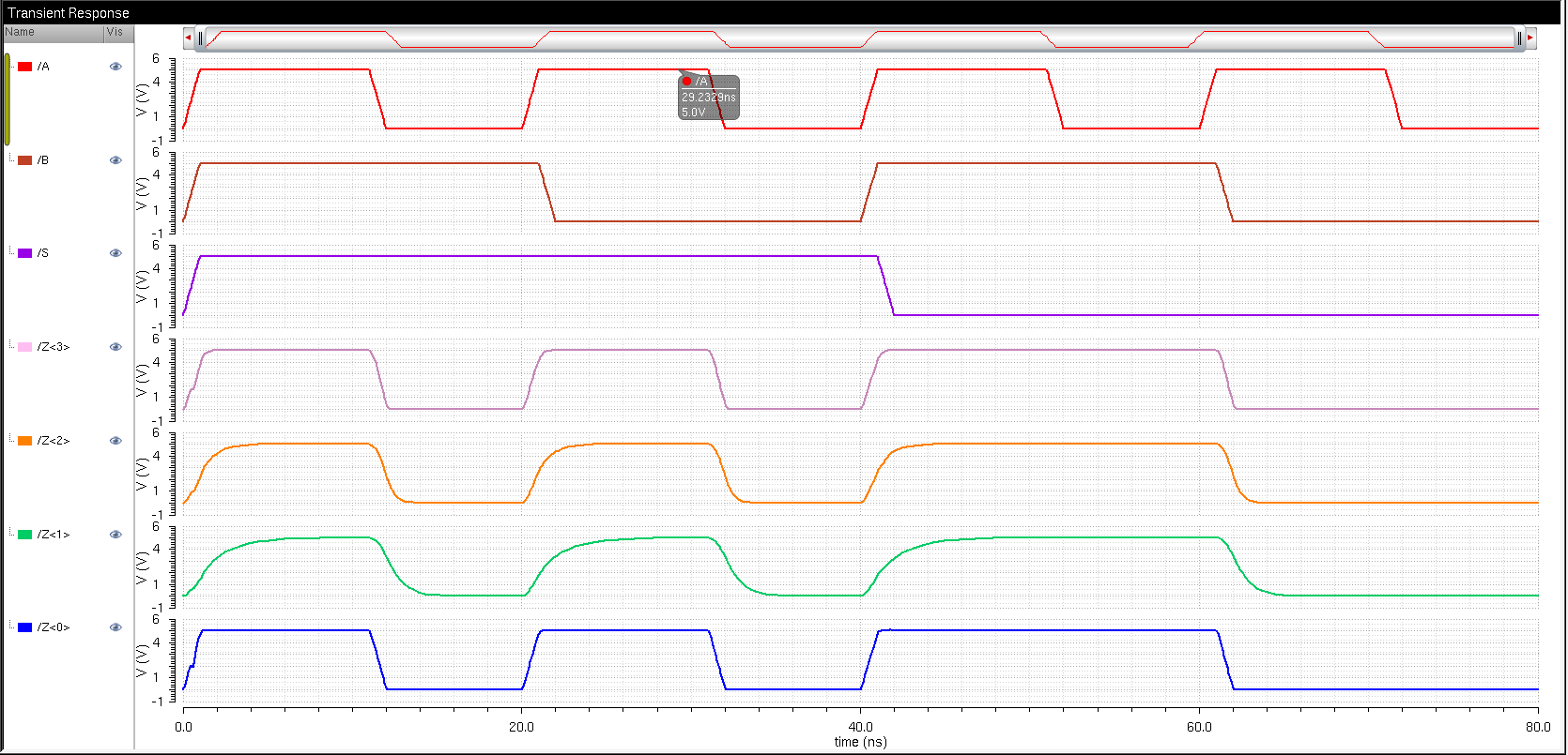 |
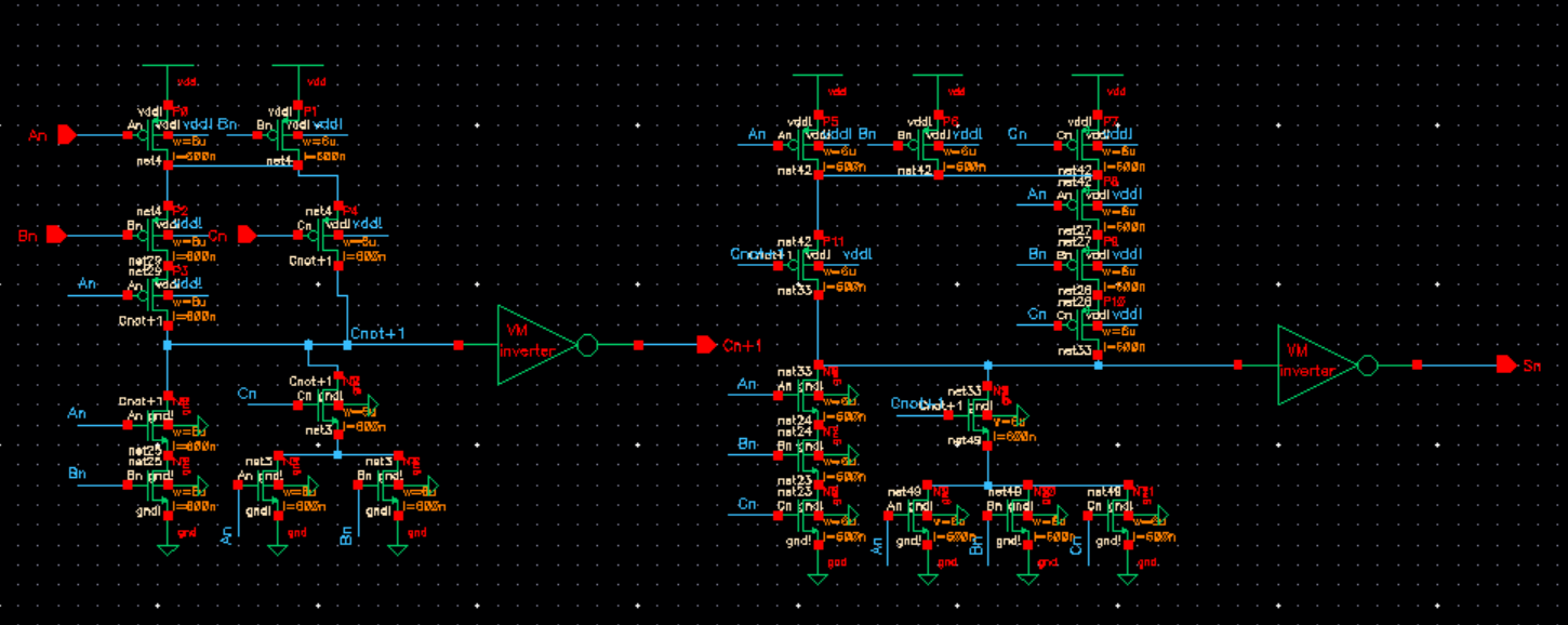
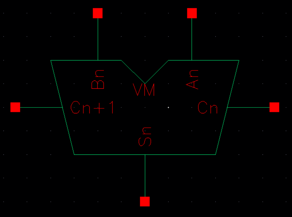
Full Adder Schematics and Layout
| Full Adder Schematic | Full Adder Symbol |
 |  |
| 8-bit Full Adder Schematic | 8-bit Full Adder Symbol |
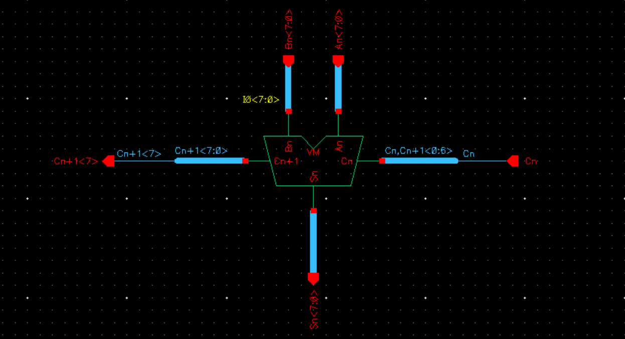 | 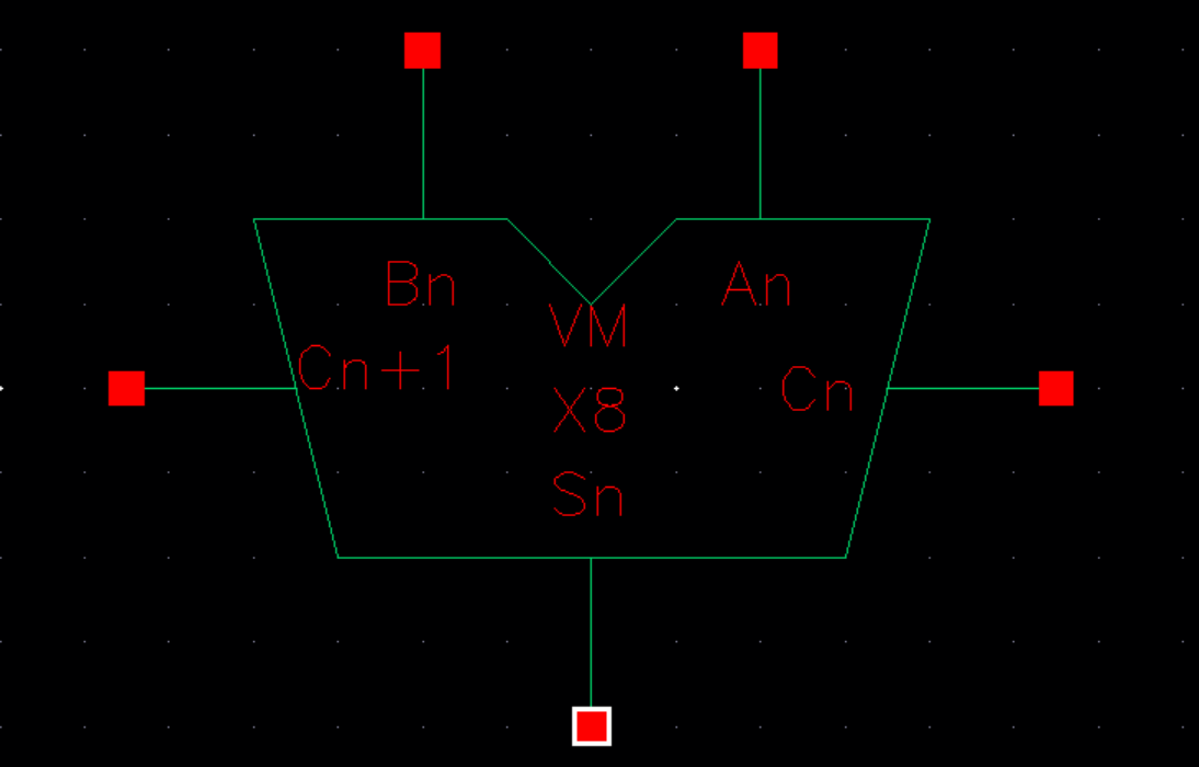 |
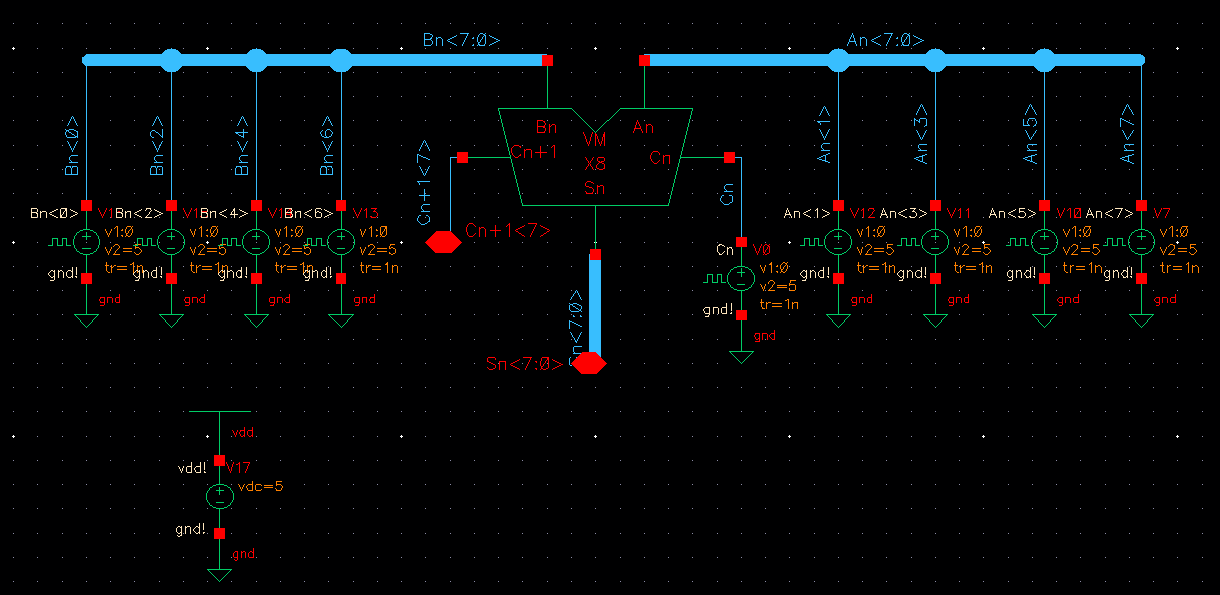
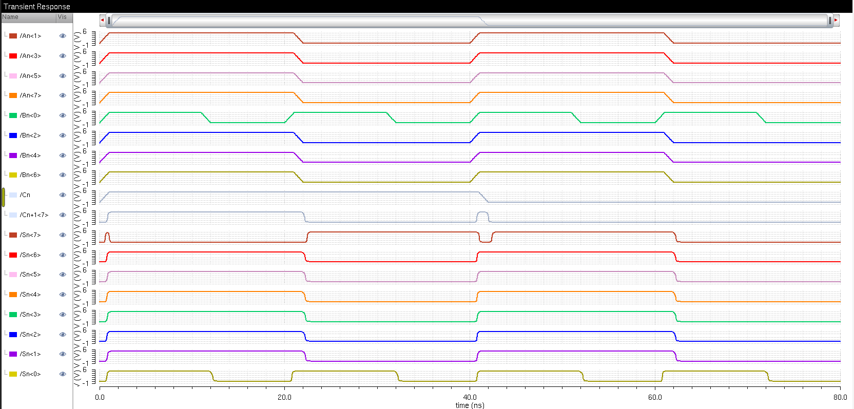
| Simulate 8-bit Full Adder | 8-bit Full Adder Plots |
 |  |
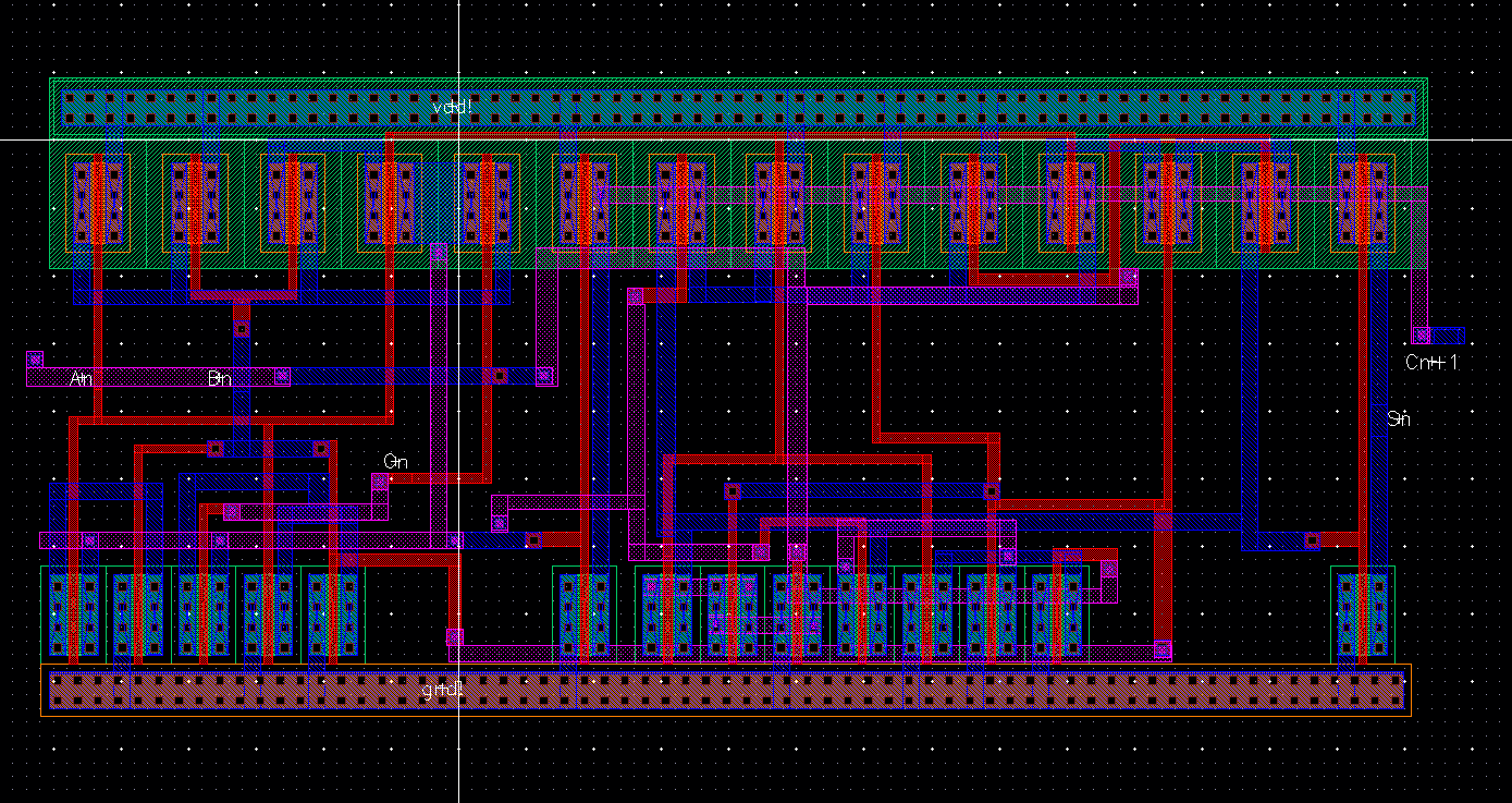
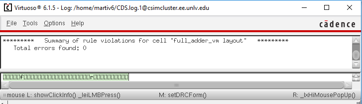
| Full Adder Layout | Full Adder DRC |
 |  |
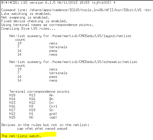
| Full Adder LVS | Full Adder Extracted |
 | 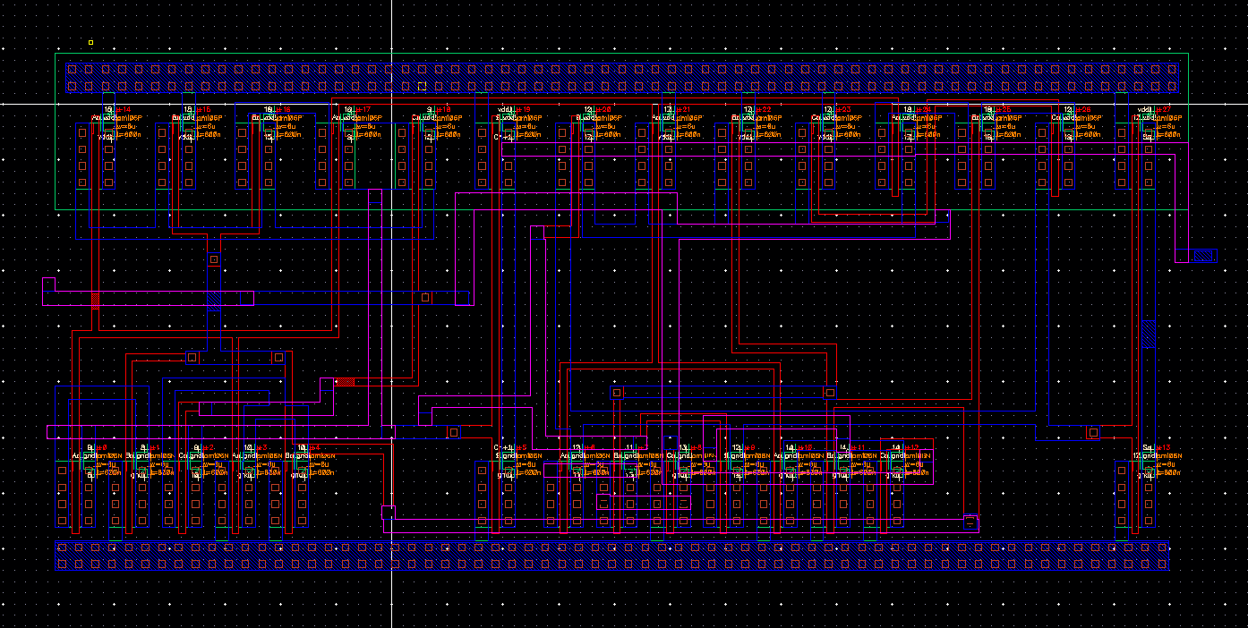 |
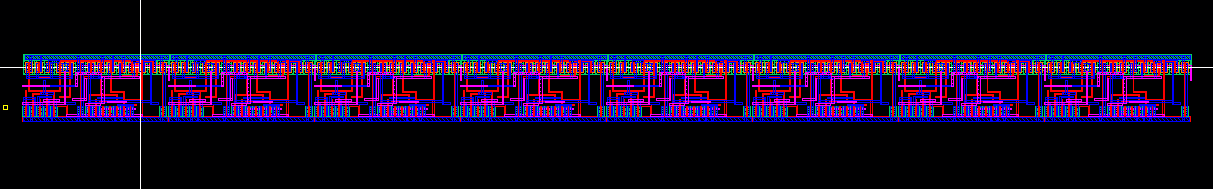
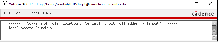
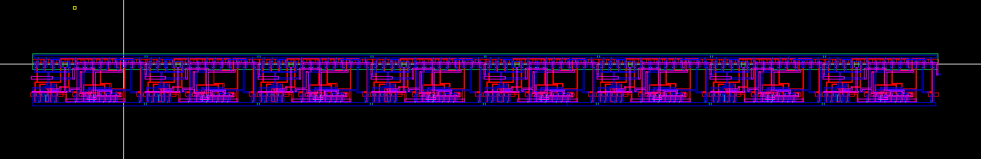
| 8-bit Full Adder Layout | 8-bit Full Adder DRC |
 |  |
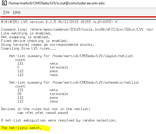
| 8-bit Full Adder LVS | 8-bit Full Adder Extracted |
 |  |
Backing up Work
Zipping up lab work and uploading on google drive
Return to Labs