Lab 6- EE 421L
Design, layout, and simulation of a CMOS NAND gate, XOR gate, and Full-Adder
Authored
by Victor Martinez
martiv6@unlv.nevada.edu
October 20, 2018
Pre-lab work
- Back-up all of your work from the lab and the course.
- Go through Cadence Tutorial 4 seen here.
- Read through the lab in its entirety before starting to work on it
Lab
description:
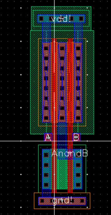
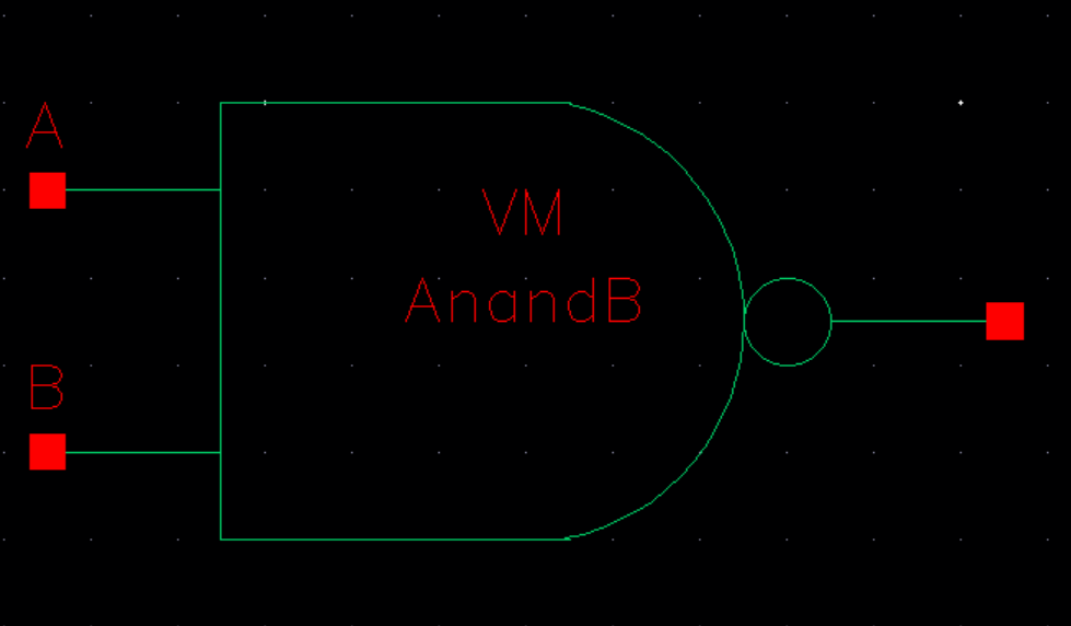
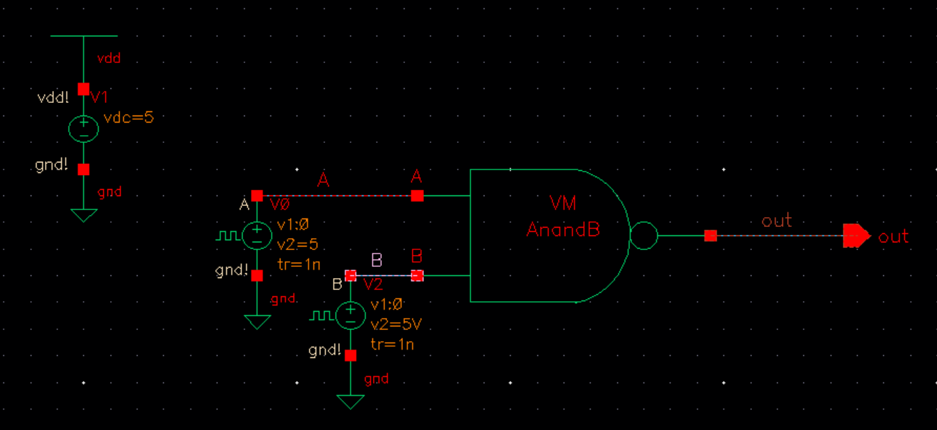
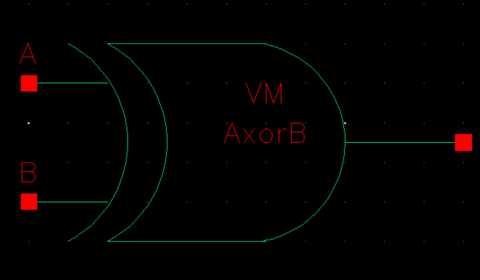
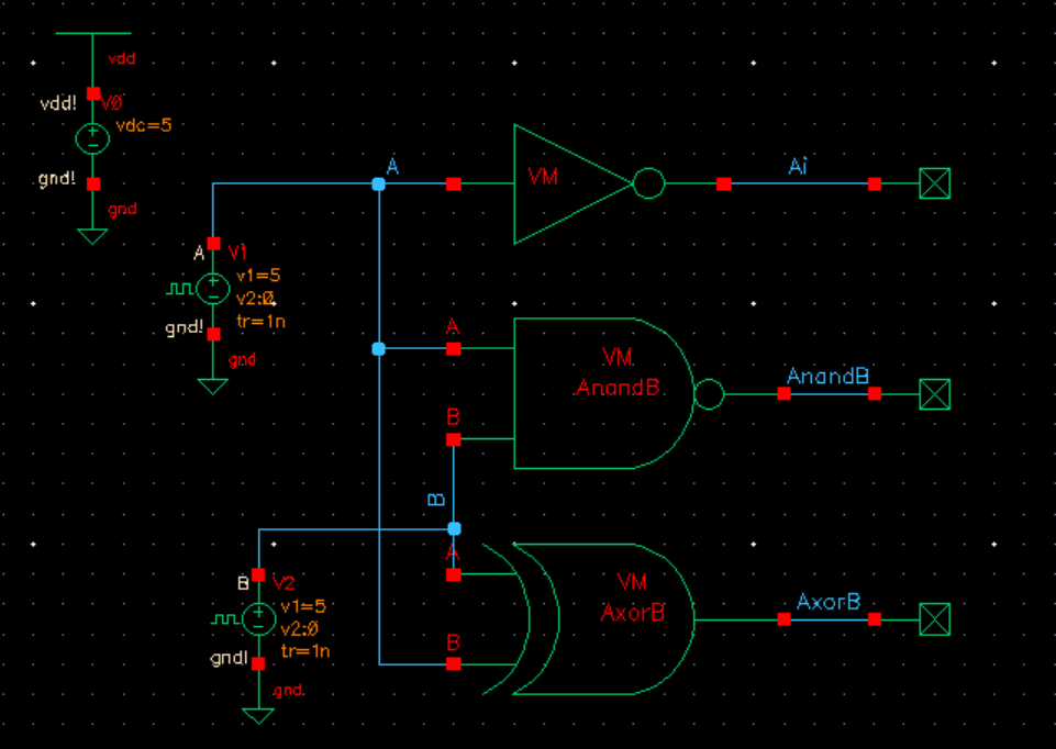
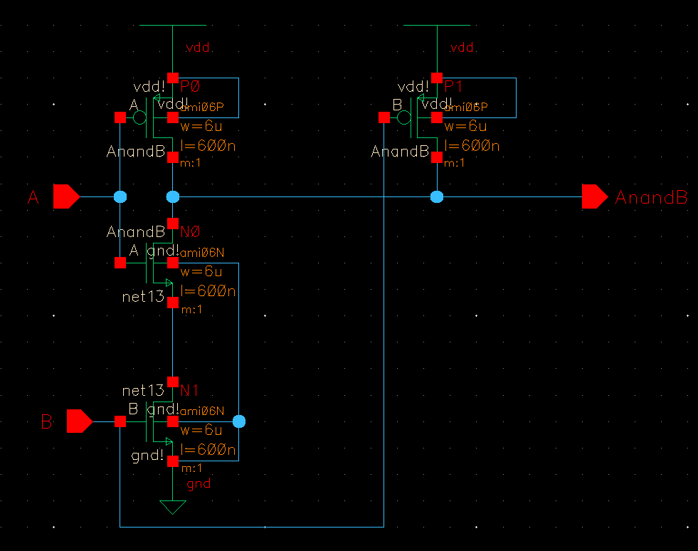
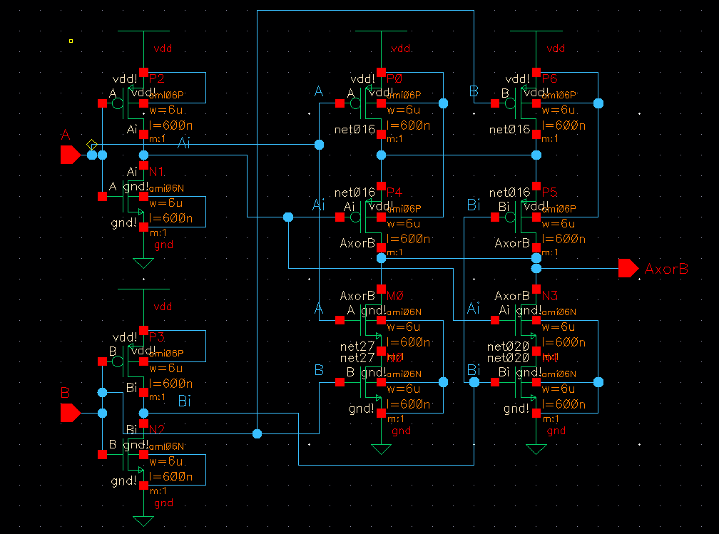
- Draft the schematics of a 2-input NAND gate, and a 2-input XOR gate using 6u/0.6u MOSFETs (both NMOS and PMOS)
NAND
XOR
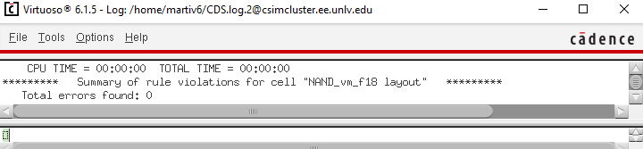
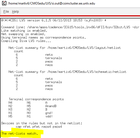
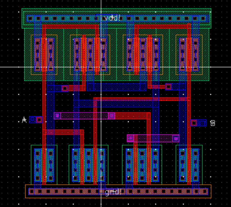
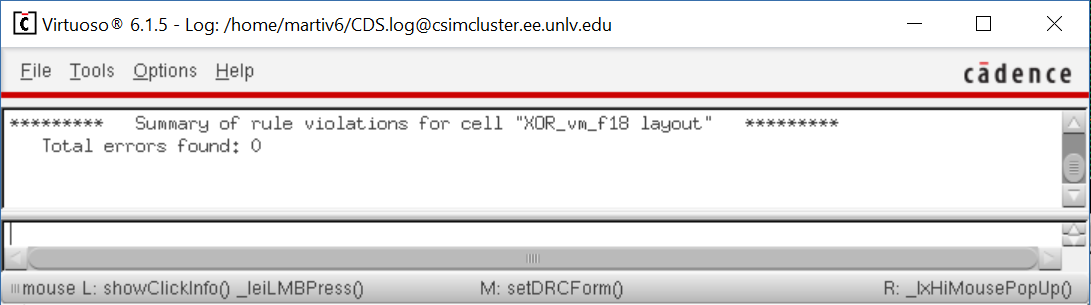
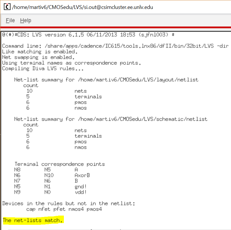
- Create layout and symbol views for these gates showing that the cells DRC and LVS without errors
NAND
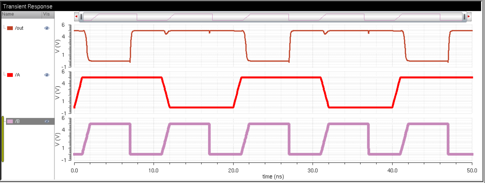
NAND Simulation
XOR
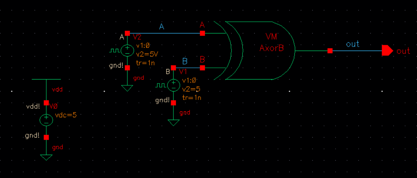
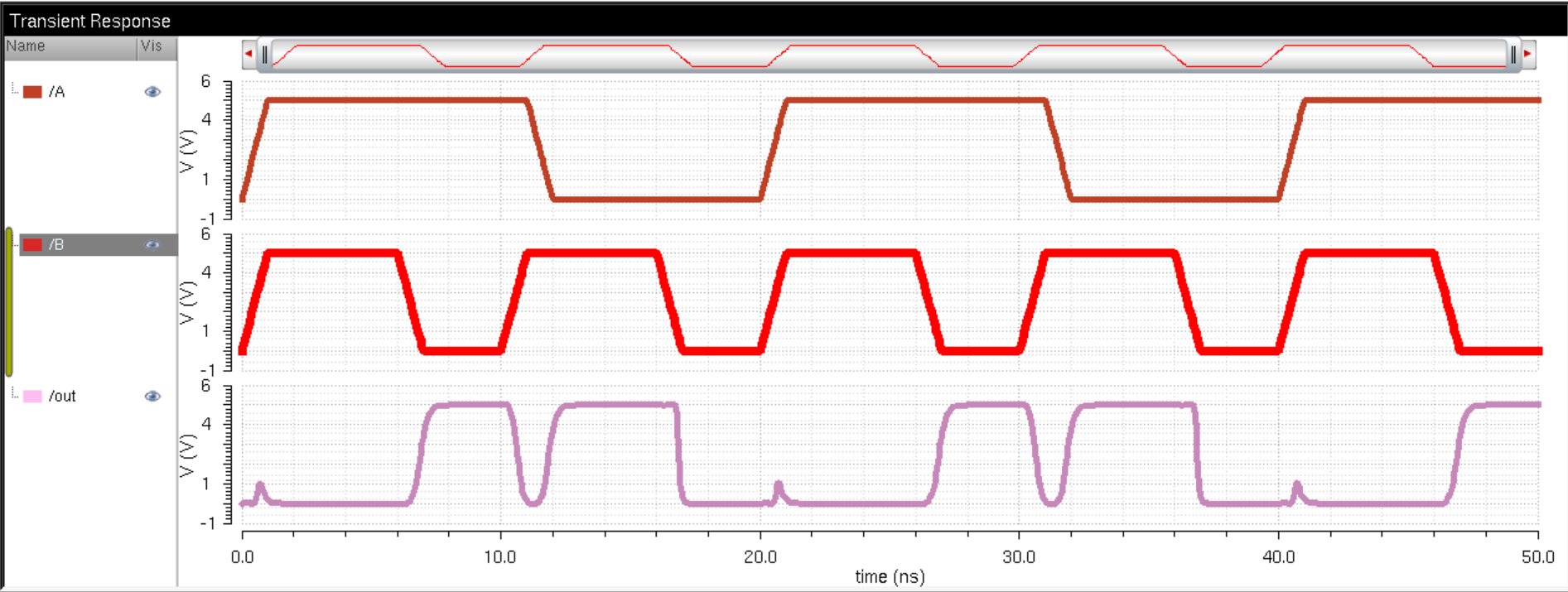
XOR Simulation
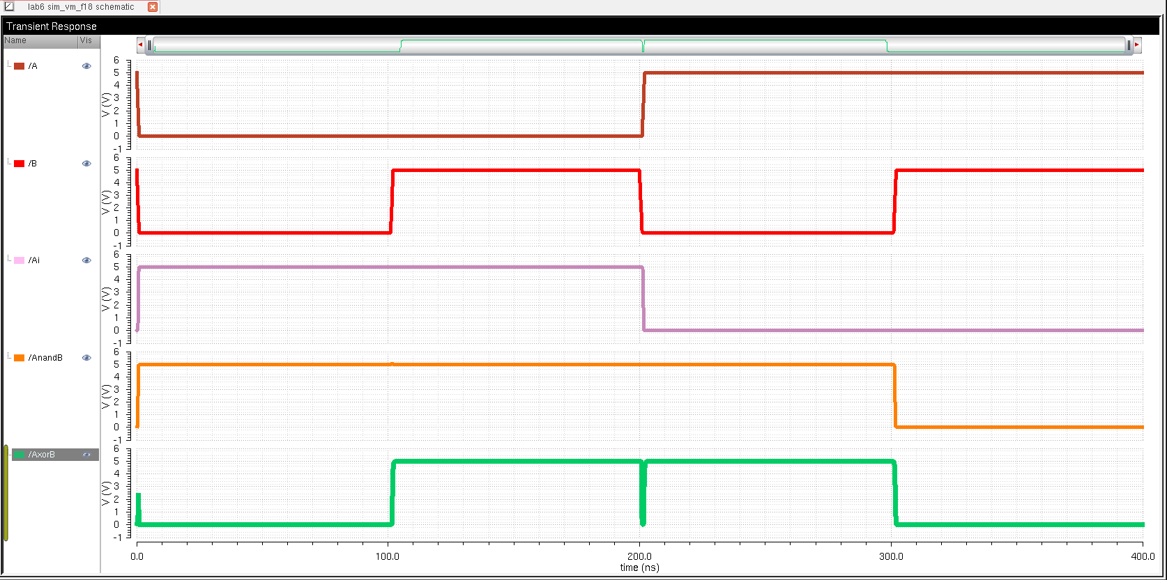
- Using Spectre simulate the logical operation of the gates for all 4 possible inputs (00, 01, 10, and 11)
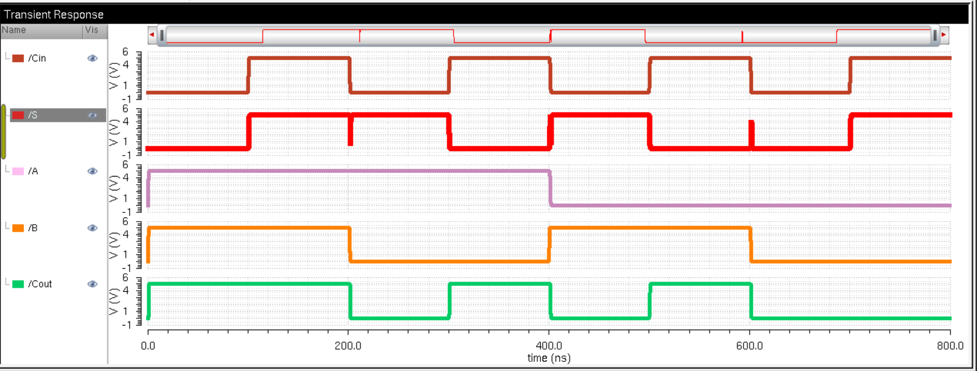
The
glitches in the NAND and XOR simulations are caused by the brief rise
and fall times of the input signals. The glitch is when the period of
the pulse is rising or falling, and the MOSFETs are neither not on or
off. If the times were decreased, the glitches wouldnt be as
noticeable. If the rise/fall time was 0 there would ne no glitch
visible.
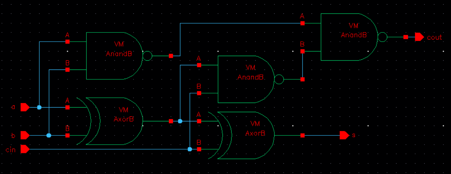
- Using these gates, draft the schematic of the full adder seen below
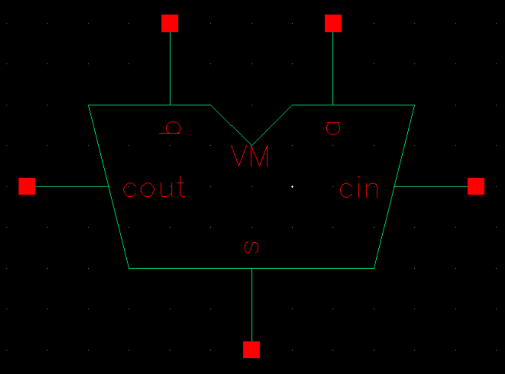
- Create a symbol for this full-adder (example)
- Simulate, using Spectre, the operation of the full-adder using this symbol
Full Adder
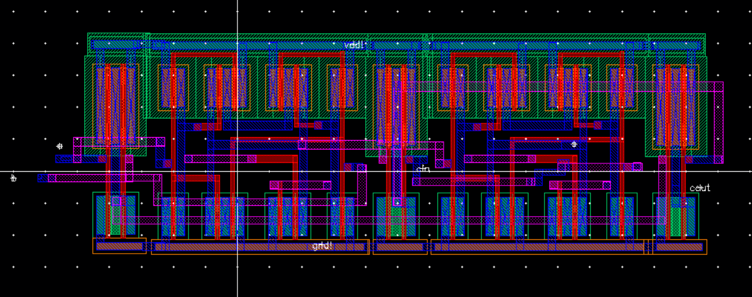
- Layout the full-adder by placing the 5 gates end-to-end so that vdd! and gnd! are routed
- full-adder inputs and outputs can be on metal2 but not metal3
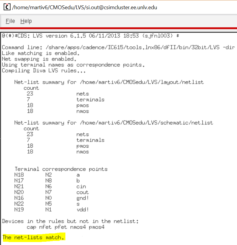
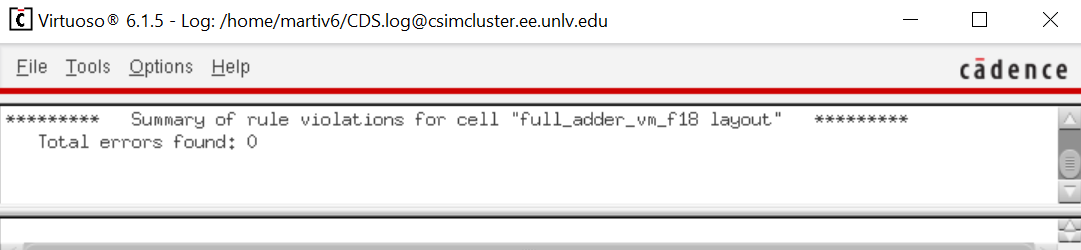
- DRC and LVS your full adder design
Full Adder
Backing up Work
Zipping up lab work and uploading on google drive
Return to Labs