Lab 4 - EE 421L
IV characteristics and layout of NMOS and PMOS devices in ON's C5 process
martiv6@unlv.nevada.edu
Pre-lab work:
Lab:
Generate 4 schematics and simulations:
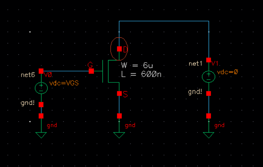
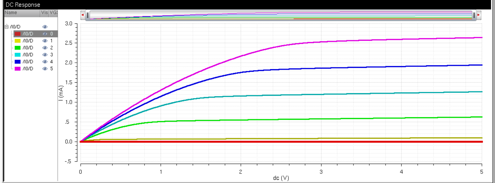
ID v. VDS of an NMOS device for
VGS varying from 0 to 5 V in 1 V steps while VDS varies from 0 to 5 V
in 1 mV steps.
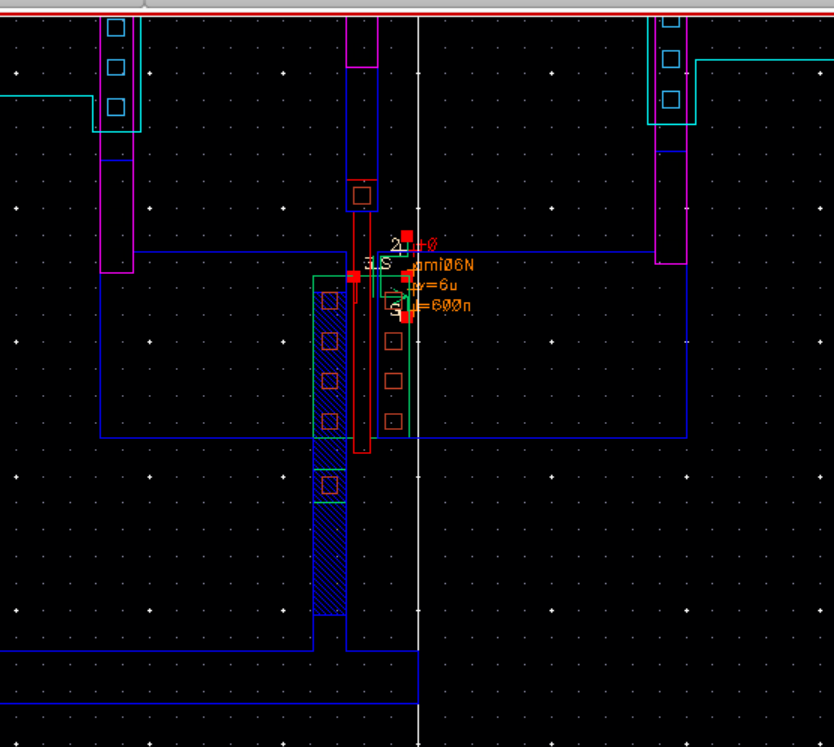
Using a 6u/600n width-to-length ratio
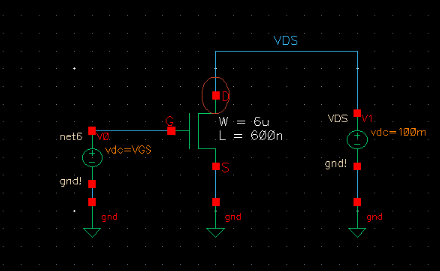
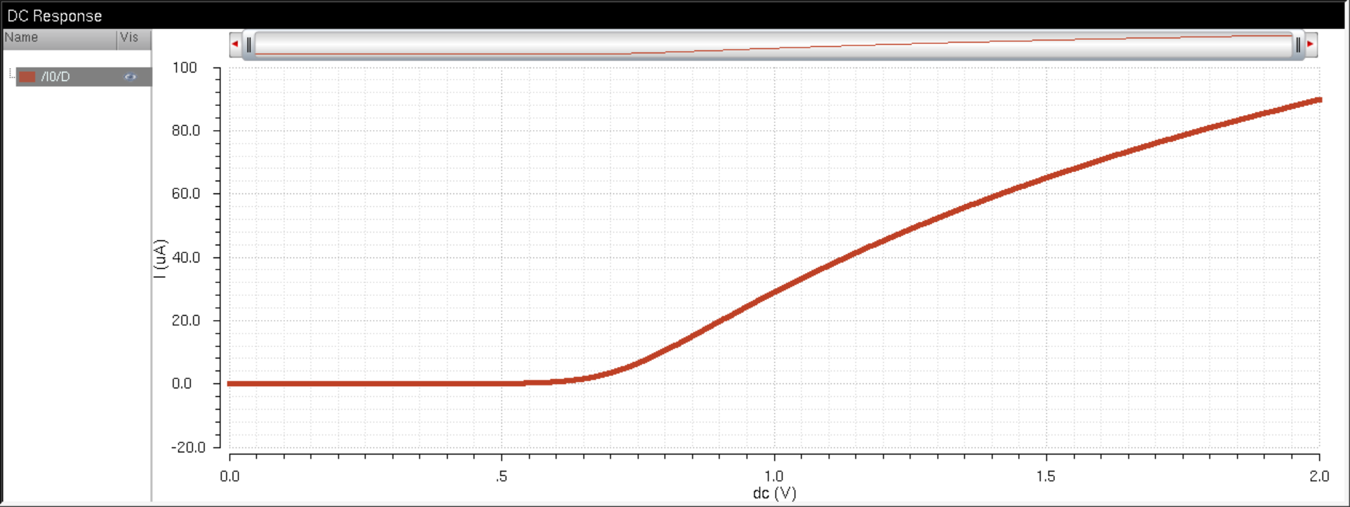
ID v. VGS of an NMOS device for VDS = 100 mV where VGS varies from 0 to 2 V in 1 mV steps.
Using a 6u/600n width-to-length ratio
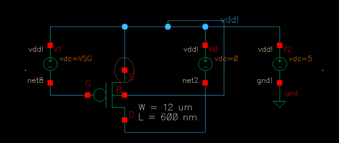
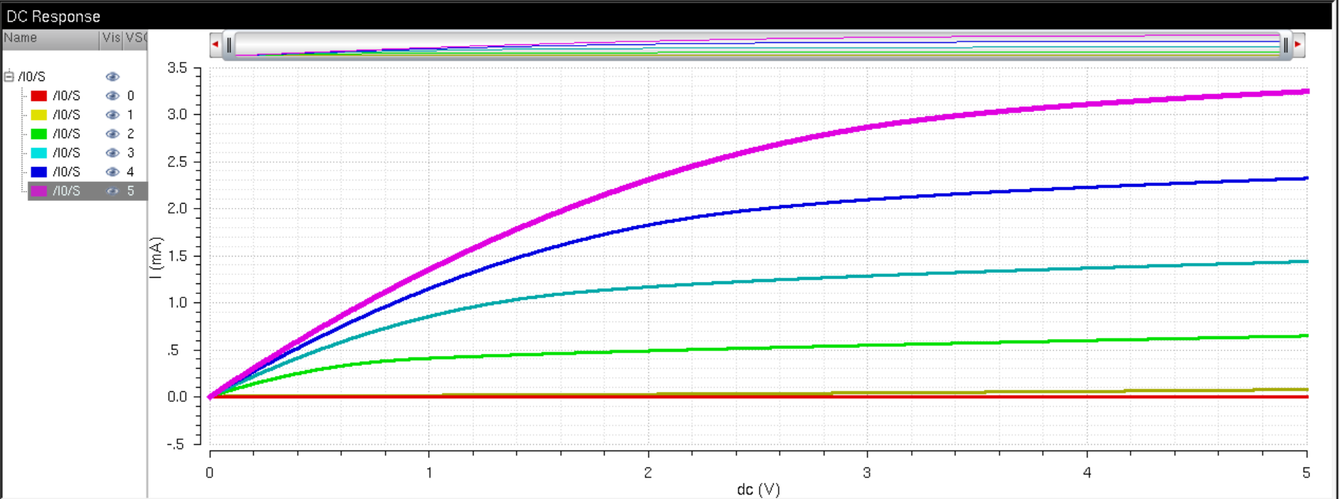
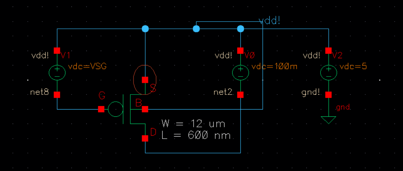
ID v. VSD (note VSD not VDS) of a PMOS device for VSG varying from 0 to 5 V in 1 V steps while VSD varies from 0 to
5 V in 1 mV steps. Using a 12u/600n width-to-length ratio.
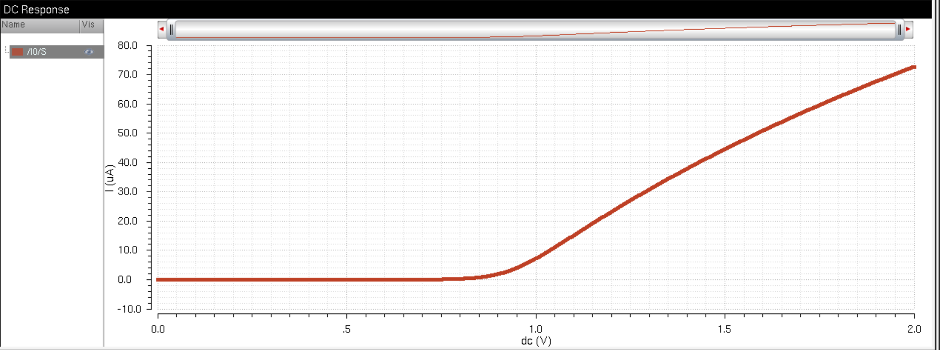
ID v. VSG of a PMOS device for VSD = 100 mV where VSG varies from 0 to 2 V in 1 mV steps.
Using a 12u/600n width-to-length ratio.
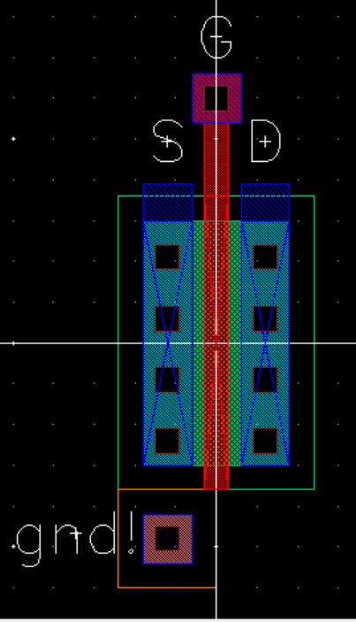
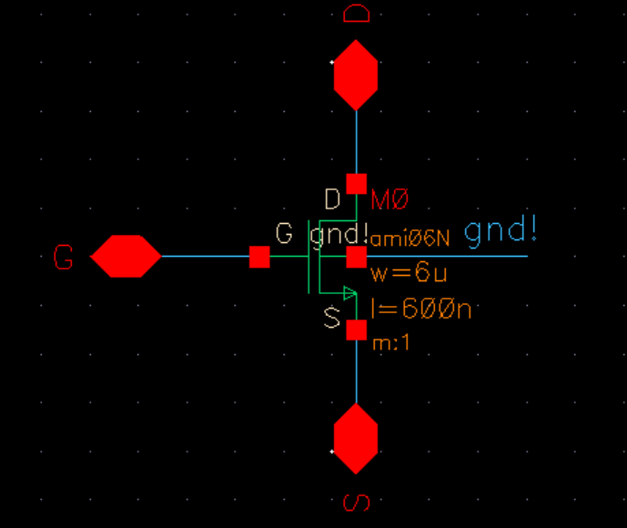
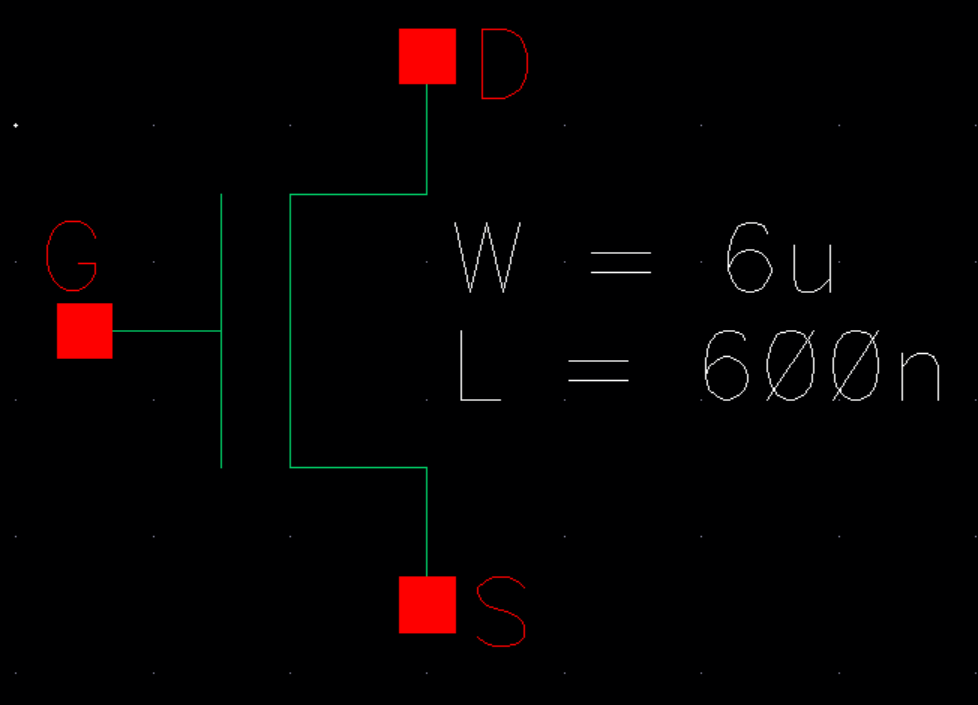
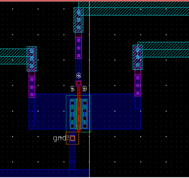
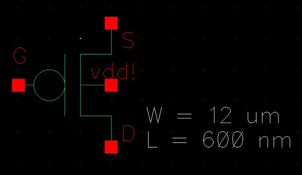
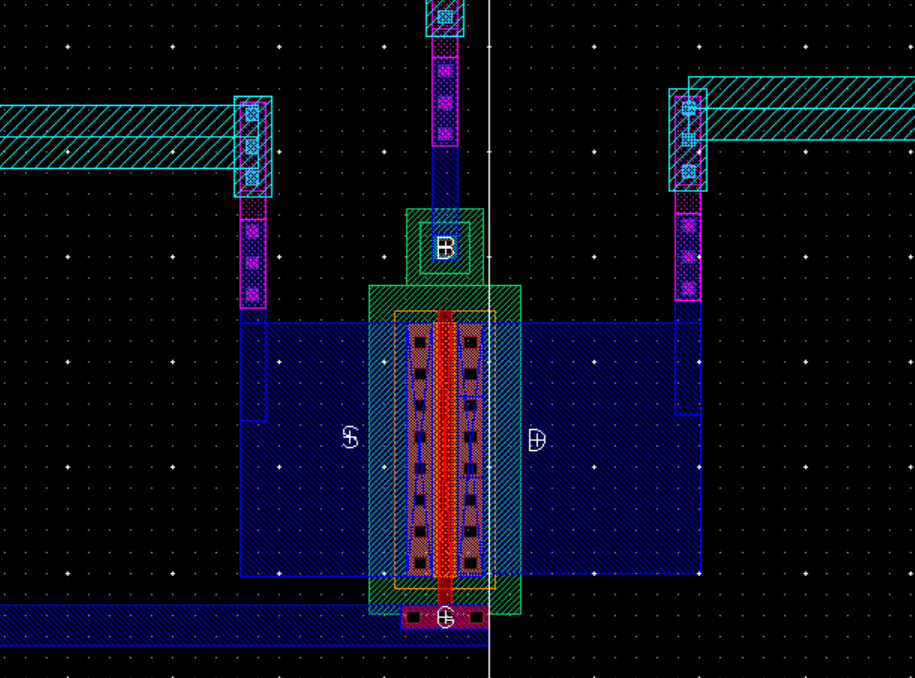
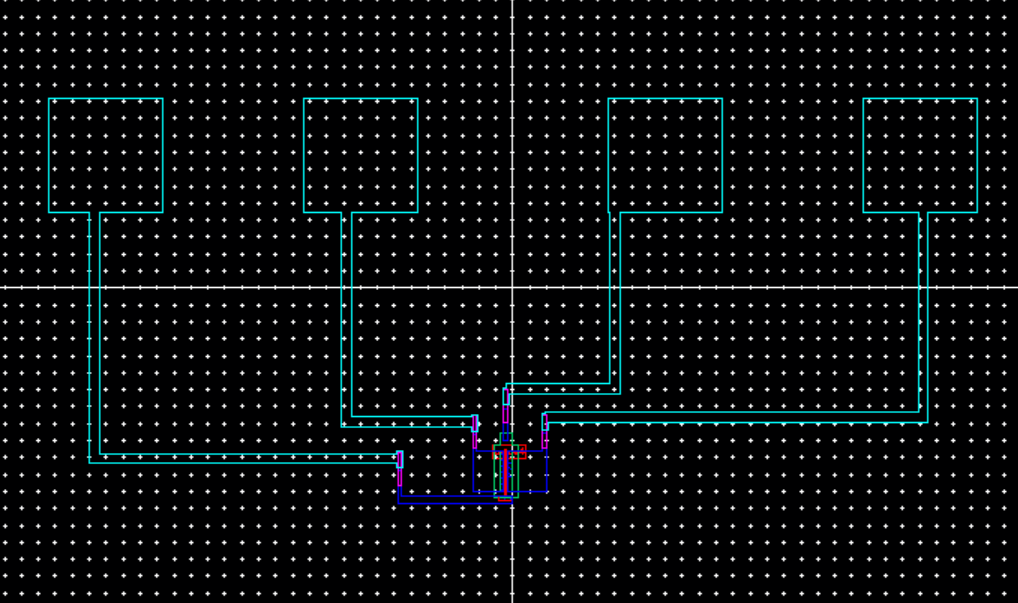
Lay out a 6u/0.6u NMOS device and connect all 4 MOSFET terminals to probe pads
Layout Extracted
Schematic Symbol
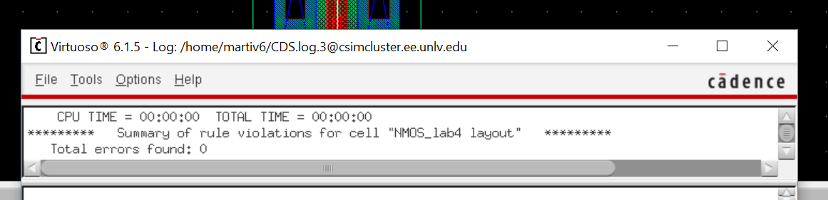
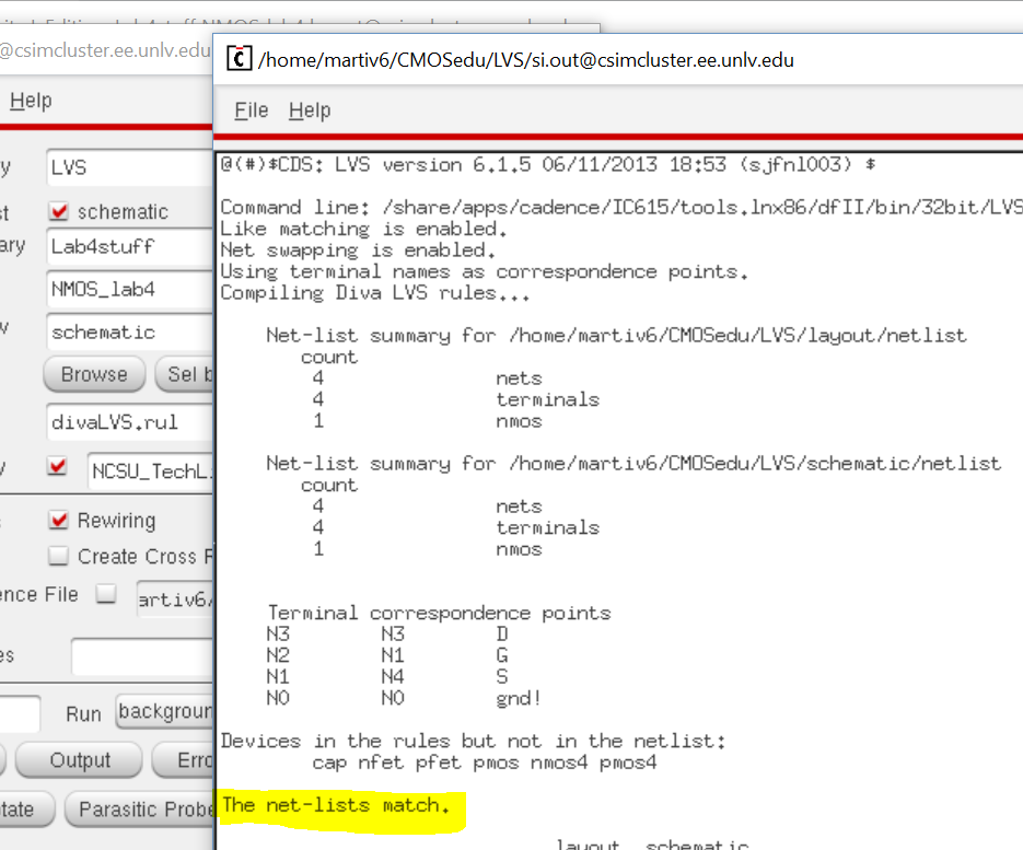
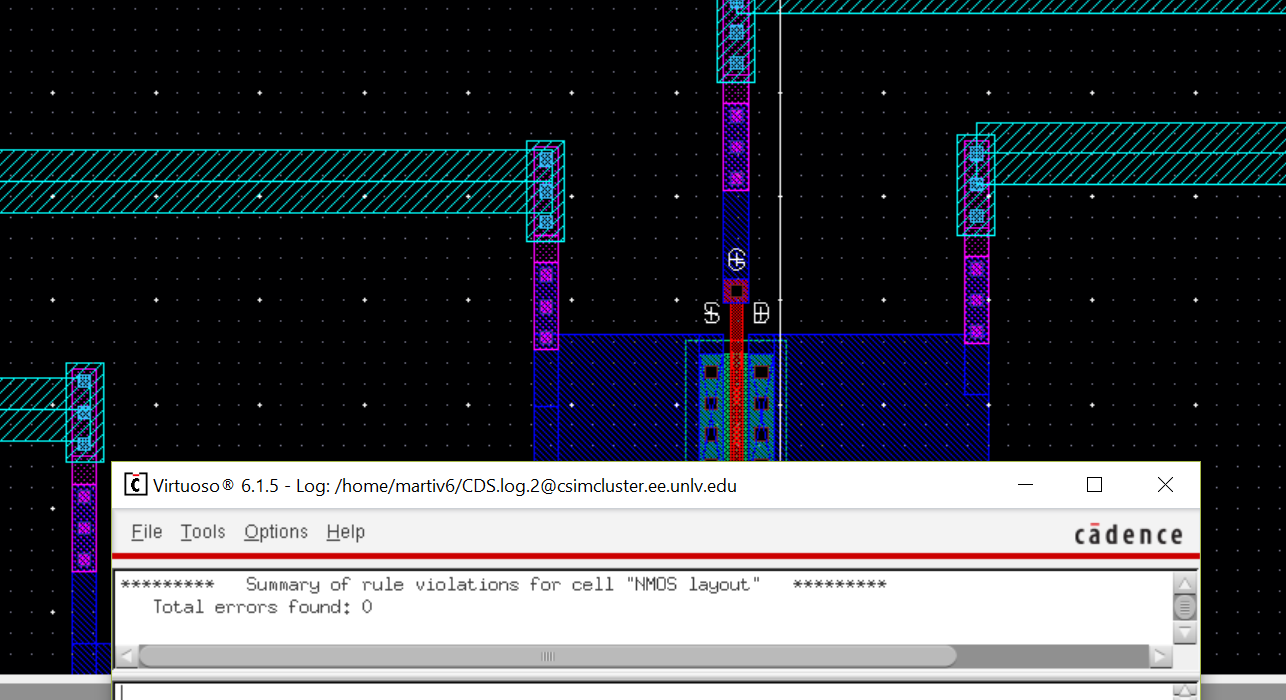
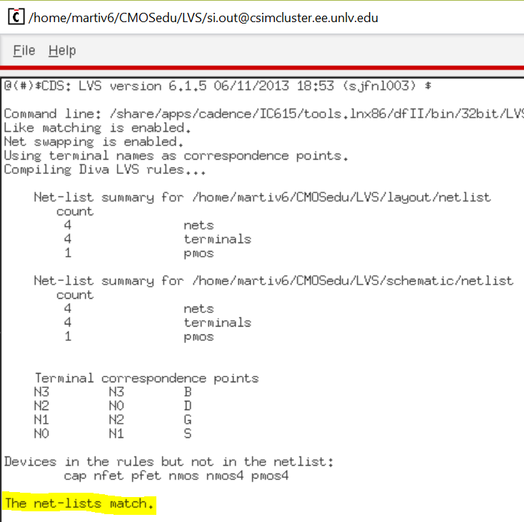
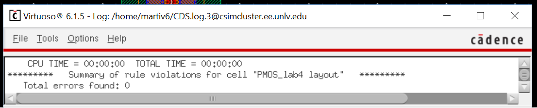
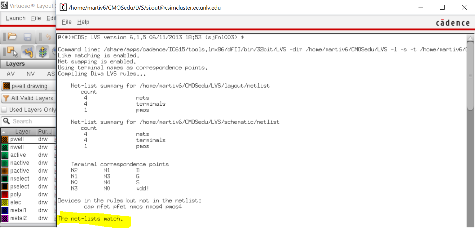
DRC and LVS
Layout with pads
Extracted
DRC and LVS of NMOS with Pads
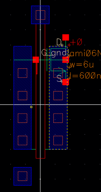
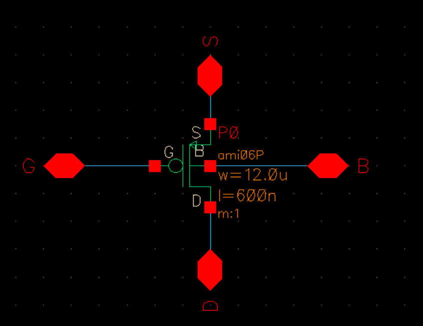
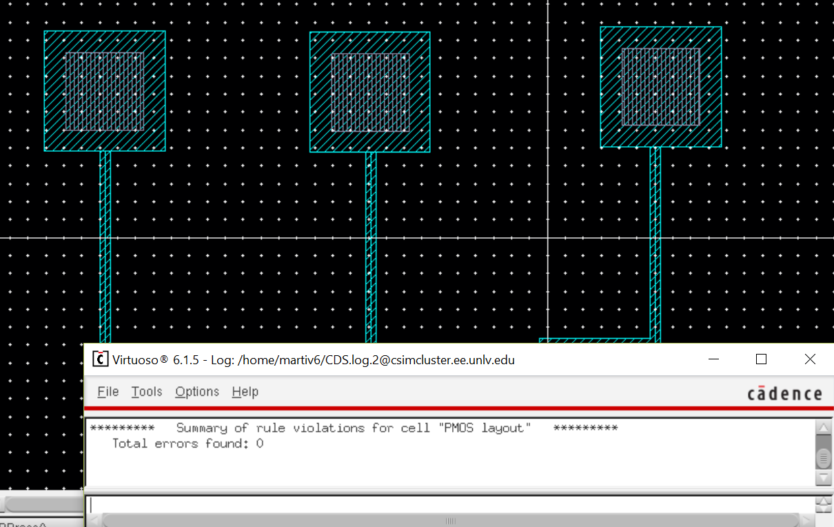
Lay out a 12u/0.6u PMOS device and connect all 4 MOSFET terminals to probe pads
Schematic Symbol
Layout Extracted
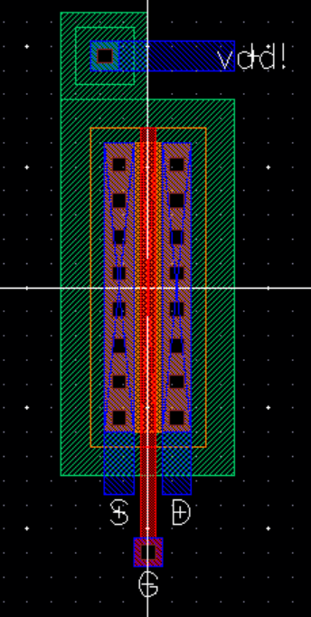
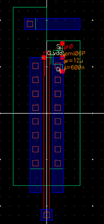
PMOS with Pads
DRC and LVS of PMOS with pads

Backing up Work
Zipping up work and putting into google drive