Lab 6 - ECE 421L
Authored
by Michael Loreto,
Email: loreto@unlv.nevada.edu
October 24, 2018
Lab
description: This lab studies the design, layout, and simulation in CMOS for the NAND gate, XOR gate, and Full Adder component.
---------------------------------------------------
Prelab Work:
- Back-up all of your work from the lab and the course.
- Go through Cadence Tutorial 4.
Tutorial 4 covers the design, layout, and simulation of a NAND gate.

Shown above are the schematics and layout for the NAND gate.

Shown here are the simulation schematic (including the created NAND symbol) and waveforms for testing out the NAND gate.
---------------------------------------------------------
Lab 6 Work:
-Draft the schematics for a 2-input NAND gate and a 2-input XOR gate using 6u/0.6u MOSFETS (both NMOS and PMOS).
-Create layouts and symbol vies for these gates, including DRC and LVS.
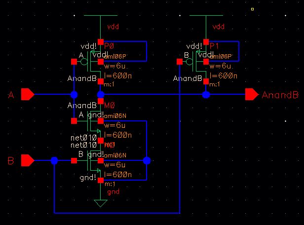
NAND Gate:
| Schematic --> |  | Symbol --> |  |
| Layout --> |  | DRC --> |  |
| Extracted --> |  | LVS --> |  |
XOR Gate:
| Schematic --> |  | Symbol --> |  |
| Layout --> |  | DRC --> |  |
| Extracted --> | 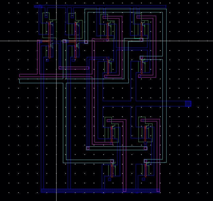 | LVS --> |  |
Note:
Despite multiple attempts to properly layout the design, the netlists
failed to match for the XOR gate. Even tried to follow the schematic
design more closely when laying out the XOR gate, but the netlists
still would not match for the layout.
----------------------------------------------
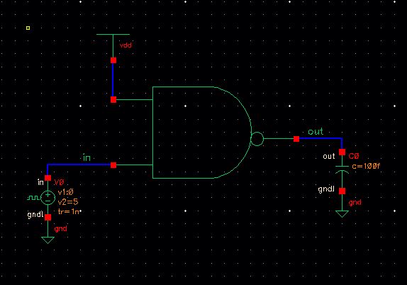
Gate Simulation Results:
| Schematic --> |  |
| Simulation --> |  |
| Comments --> | Glitches
are present in the NAND and XOR gate sims due to rise and fall times
from the input signals. Since there is a delay between these rise and
fall times, this causes the output to show a spike or a dip due to the
state of the MOSFETs, as they are neither on nor off for this brief
period of time. The smaller the delay for the rise and fall time, the
more ideal the output signal will be. |
--------------------------------------------------------------
Full-Adder:
| Inner Schematic |  |
| Simulation Schematic |  |
| Symbol |  |
| Simulation |  |
Layout & Extracted:


-----------------------------------------------------
Full Adder DRC / LVS:


Note:
I had a similar issue with the LVS on the full adder layout. After
multiple attempts to fix the mismatching on both the layout and
schematic, I still could not pinpoint the exact problem. I wired all
the components and layouts to the best of my ability, even following
the given schematics side-by-side to hopefully fix the issue.
--------------------------------------------------------------
Add
a return to the listing of your labs