Lab 3 - EE 421L 

Authored by Brian Medrano Kiaer

E-mail: kiaer@unlv.nevada.edu

September 17th 2018


Prelab work:

- Finish Tutorial 1

http://cmosedu.com/jbaker/courses/ee421L/f18/students/kiaer/lab3/snip1.JPG

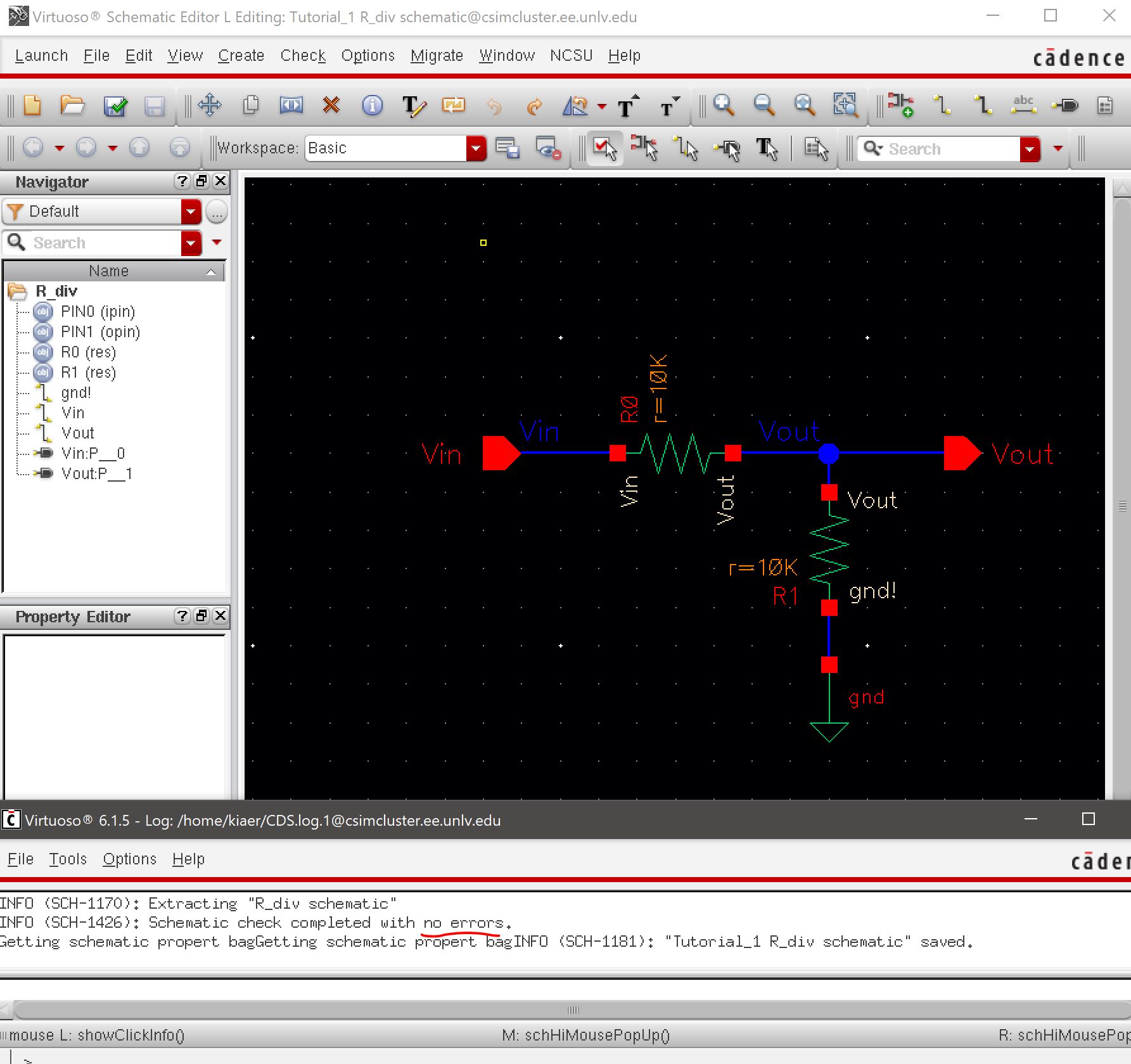
First is to create a a new cell within the Tutorial 1 Library called "R_div" this will be in the schematic view.

http://cmosedu.com/jbaker/courses/ee421L/f18/students/kiaer/lab3/snip2.JPG

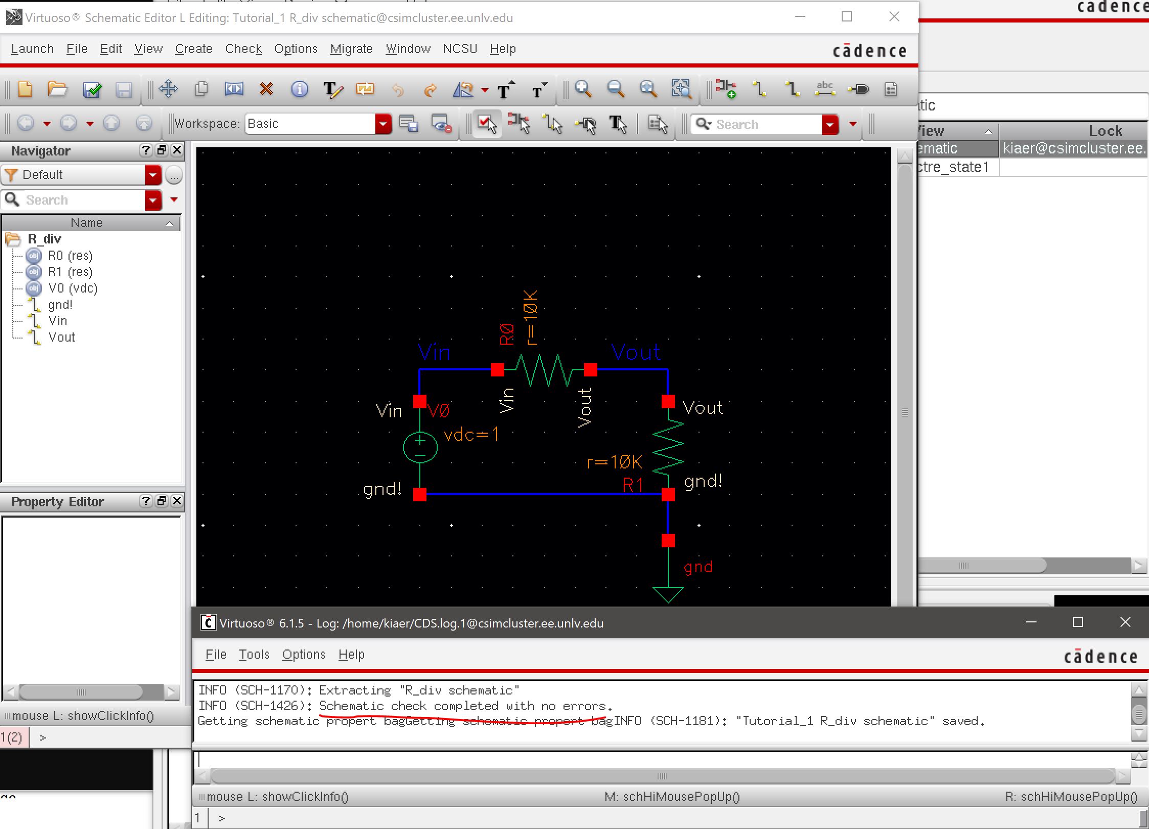
After creating the voltage divider, it is imperative to "check and save" the file on the top left of the Schematic Editor. Above we can see in the log that the schematic check has completed with no erros and the schematic has been saved.

http://cmosedu.com/jbaker/courses/ee421L/f18/students/kiaer/lab3/snip3.JPG

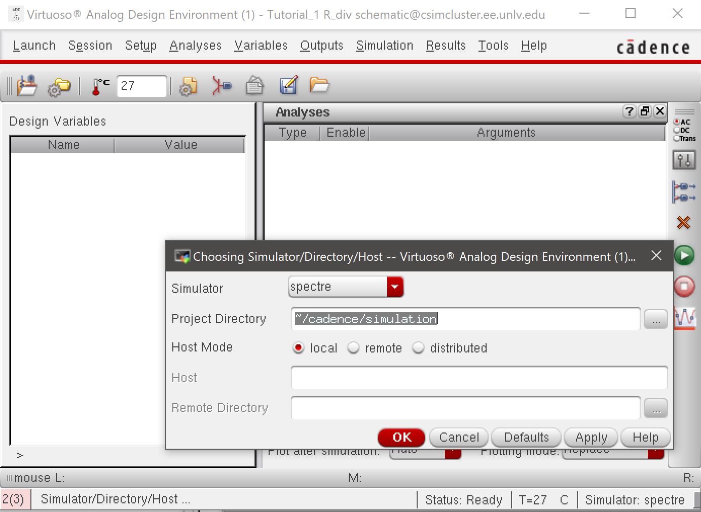
Next is to simulate the schematic that has been created as R_div. First is to open the Virtuoso Analog Design Environment (ADE) by clicking on Launch->ADE L. Then once ADE opens, next is to press Setup->Simulator/Directory/Host and ensure that "spectre" has been chosen by default in the Simulator drop down menu.

http://cmosedu.com/jbaker/courses/ee421L/f18/students/kiaer/lab3/snip4.JPG

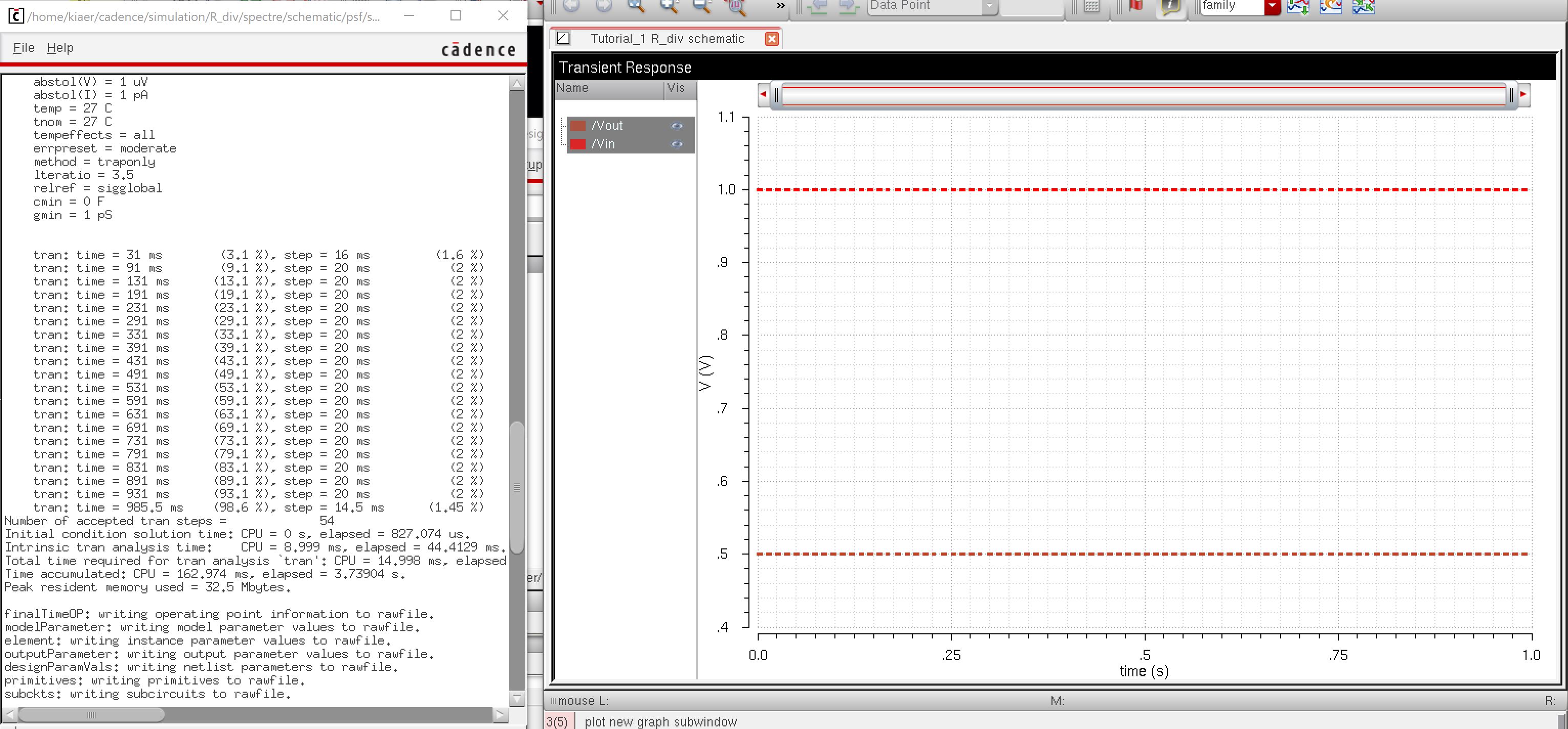
After simulation this should be the desired output of the Voltage Divider. With Vout approximately half of Vin. This simulation was created by pressing on Analyses->Choose and then selecting "tran", entering stop time "1", and checking the "enabled" box. Before simulating, be sure to save the state in cellview for access to the simulation again at a later date.

http://cmosedu.com/jbaker/courses/ee421L/f18/students/kiaer/lab3/snip5.JPG

The next step is to create a symbol of the schematic above. To create the schematic above, I removed the voltage source and the bottom connecting wires and added pins to the input and the output (bindkey P or Create->Pin). After doing so, I checked and saved to ensure that schematic is thoroughly correct.

http://cmosedu.com/jbaker/courses/ee421L/f18/students/kiaer/lab3/snip6.JPG

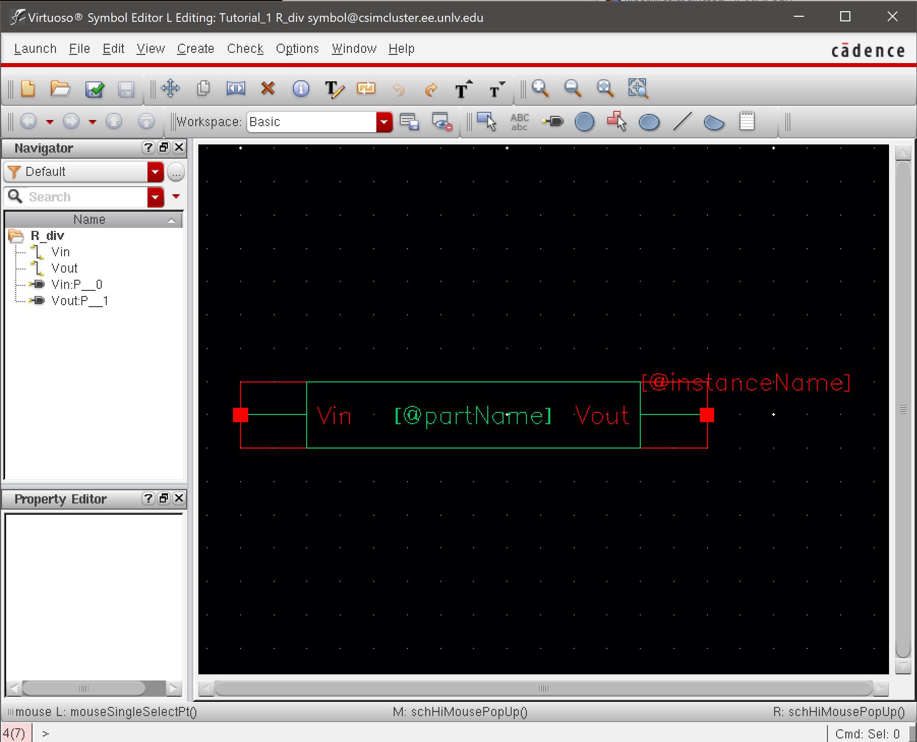
Next I created a symbol of the R_div schematic by selecting Create->Cellview->From CellView and then hit OK twice. Once that has been done, the symbol appears like the image above.

http://cmosedu.com/jbaker/courses/ee421L/f18/students/kiaer/lab3/snip7.JPG

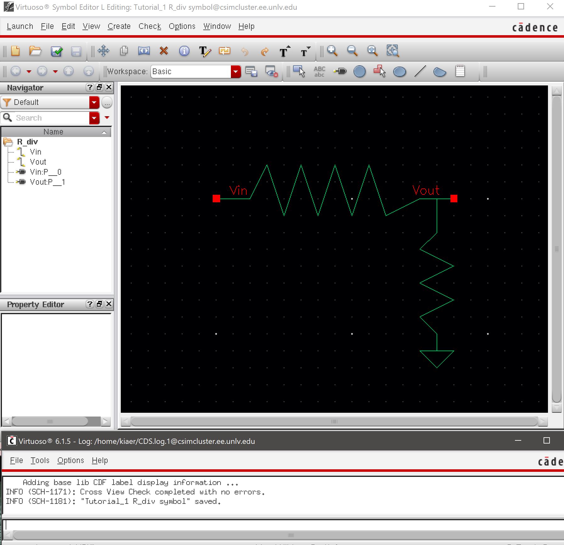
Then I deleted the other lines that were not "Vin" or "Vout" and created a symbol that resembled the voltage divider schematic. I used Create->Shape->Line to make it look like resistors were connected. Once that was done, I checked sand saved to ensure no errors occured.
http://cmosedu.com/jbaker/courses/ee421L/f18/students/kiaer/lab3/snip8.JPG

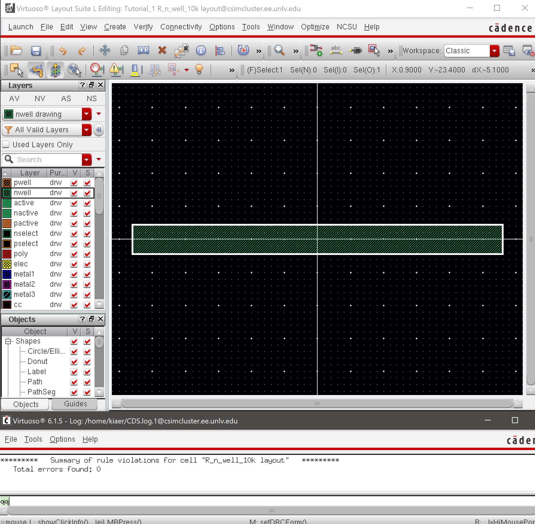
Next is to create a layout called R_n_well_10k. For the 10k resistor.  
10k/800 Ohms = 12.5 or approx 12 lambda.
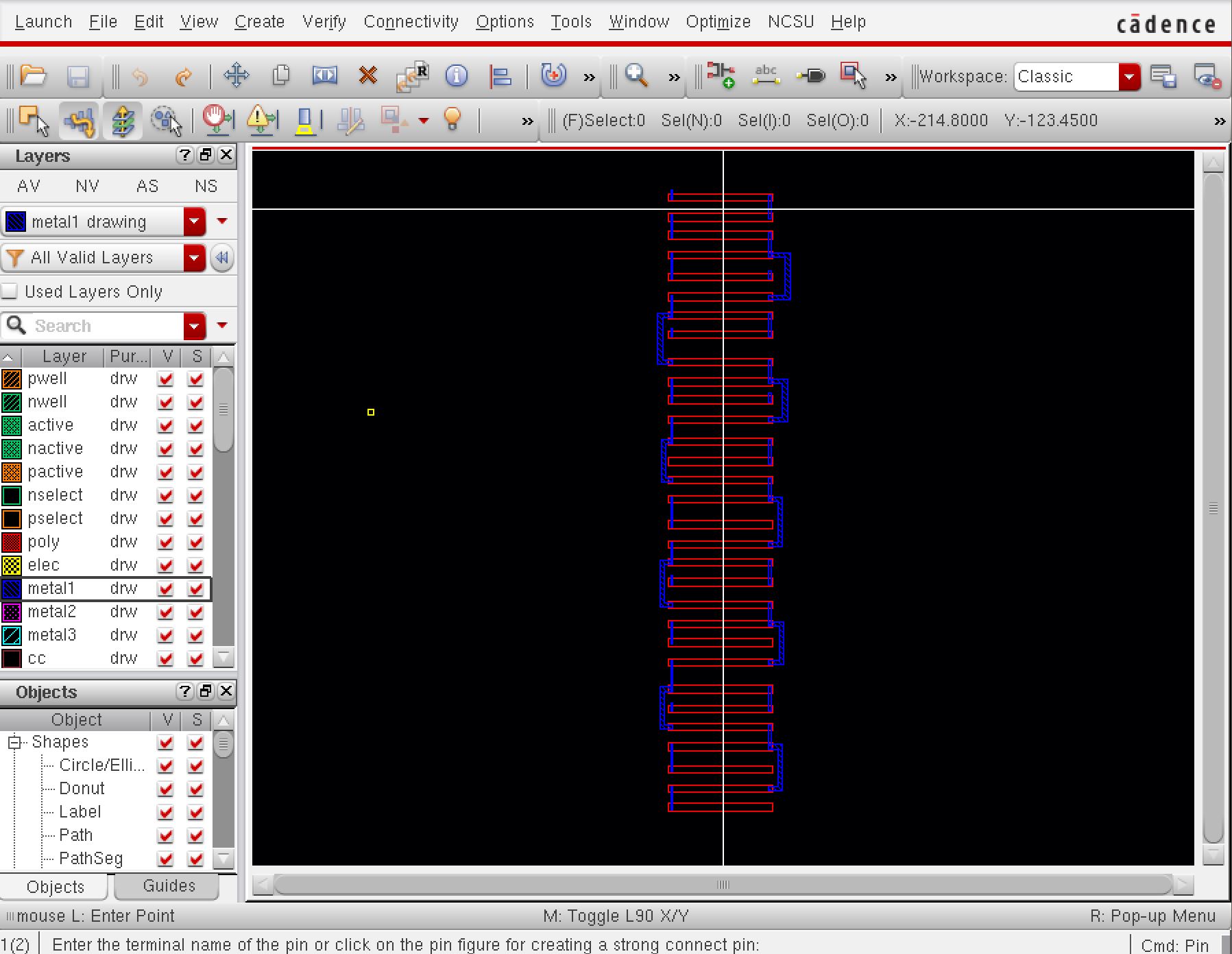
if we use a width of 4.5 um then then length would be approx 56 um. I used 56.1 to ensure that it would fit on the grid. (within 0.15) If it did not fit, the DRC check would give 4 errors since it does not fit on the grid. After this, the metal1 connections are added to both sides of the n-well and the res_id layer is added on to the original rectangle (4.5 um x 56.1 um)

http://cmosedu.com/jbaker/courses/ee421L/f18/students/kiaer/lab3/snip9.JPG


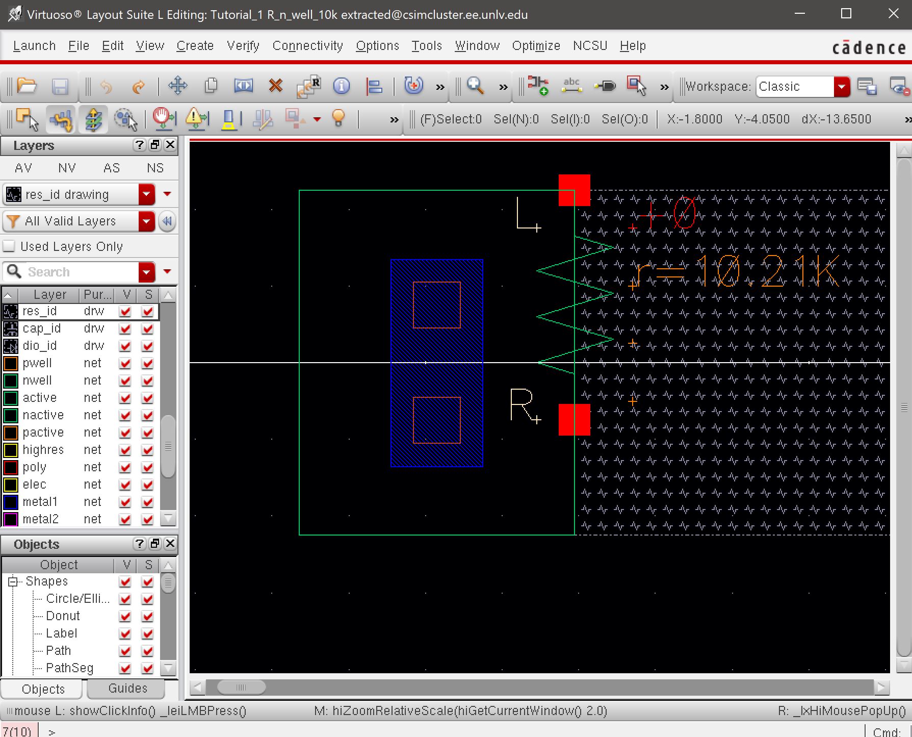
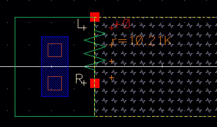
After creating the 10k N-Well Layout, I then extracted the layout (Verify->Extract) and then opened that file within the Library Manager to ensure that the output is approximately 10k.
http://cmosedu.com/jbaker/courses/ee421L/f18/students/kiaer/lab3/snip10.JPG

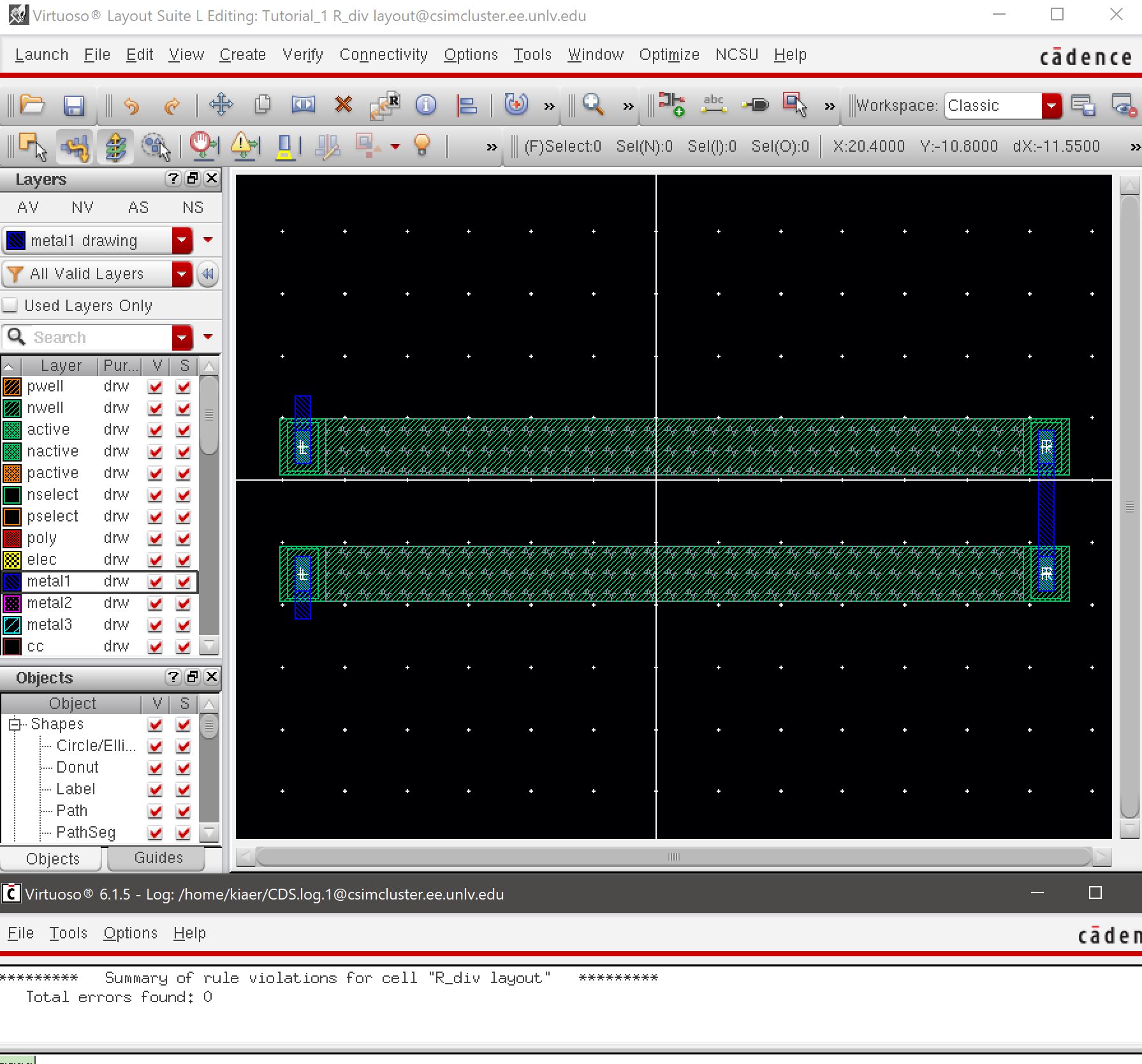
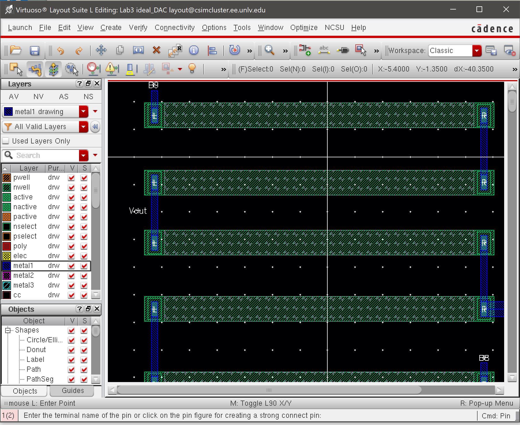
Above is the layout for R_div, I instantiated the 10k resistor layouts and connected them using the metal1 drw layer. Then I verified the DRC to ensure there were no errors. Originially I had an error due to too small of a spacing between the two resistors.

http://cmosedu.com/jbaker/courses/ee421L/f18/students/kiaer/lab3/snip11.JPG

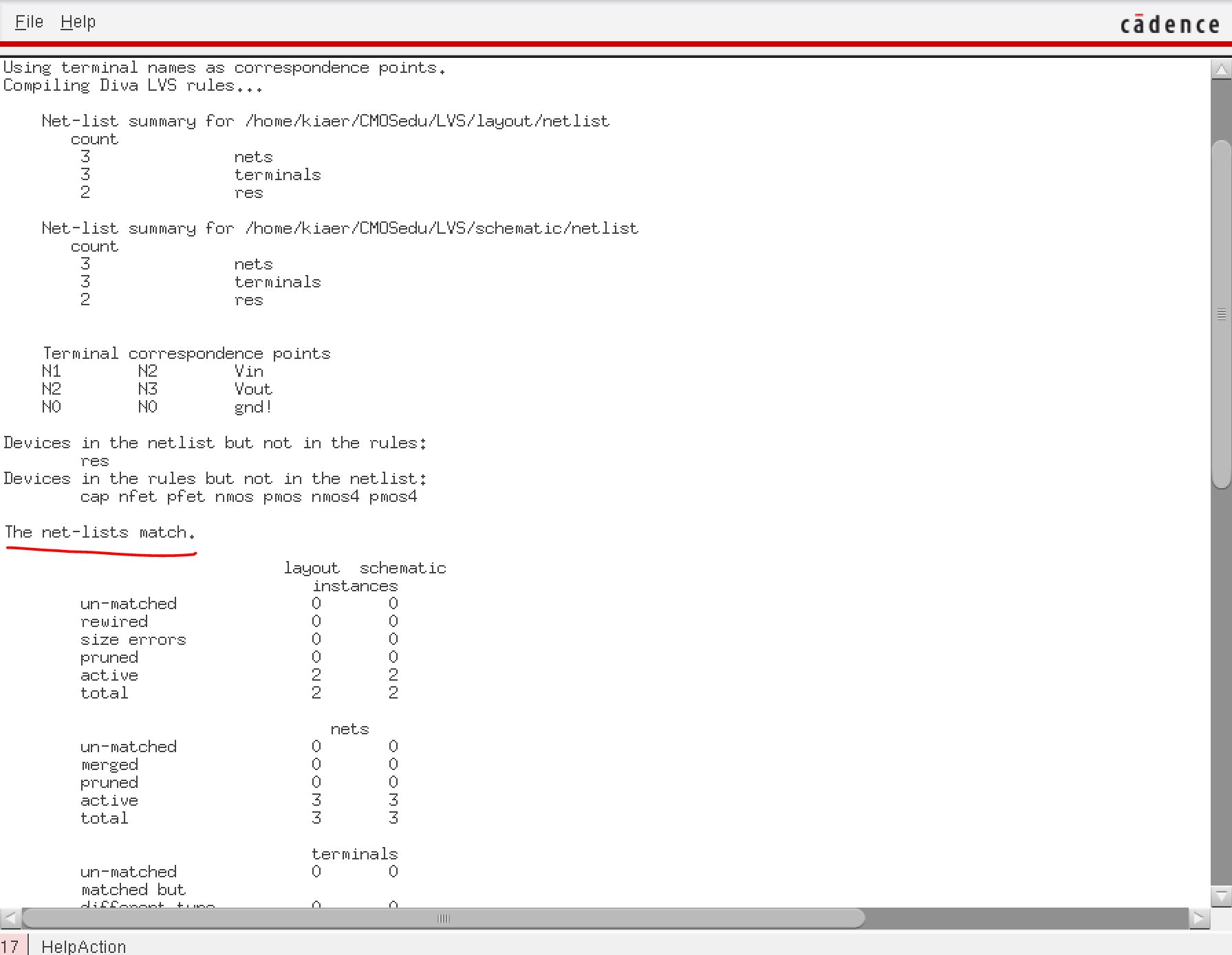
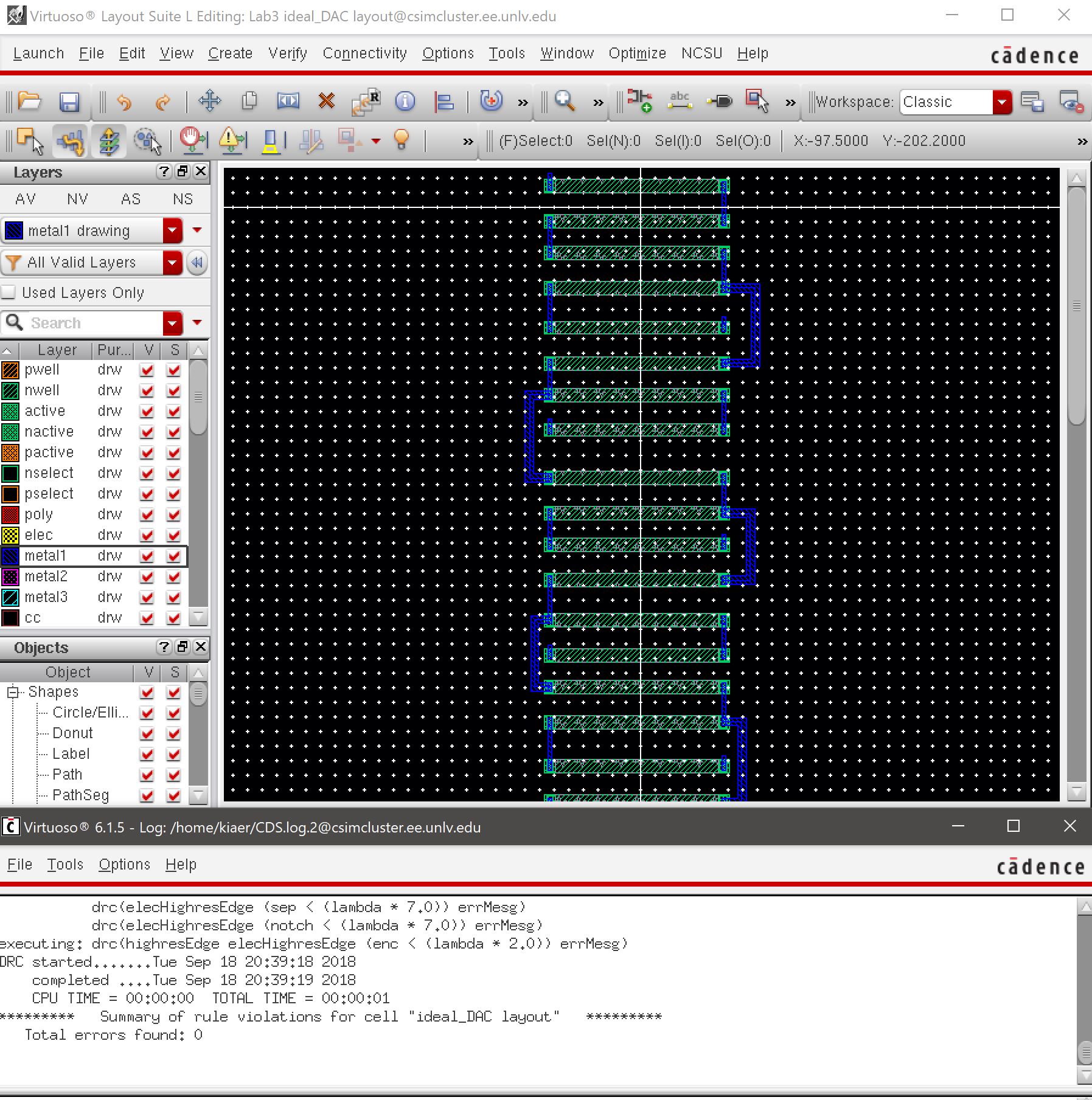
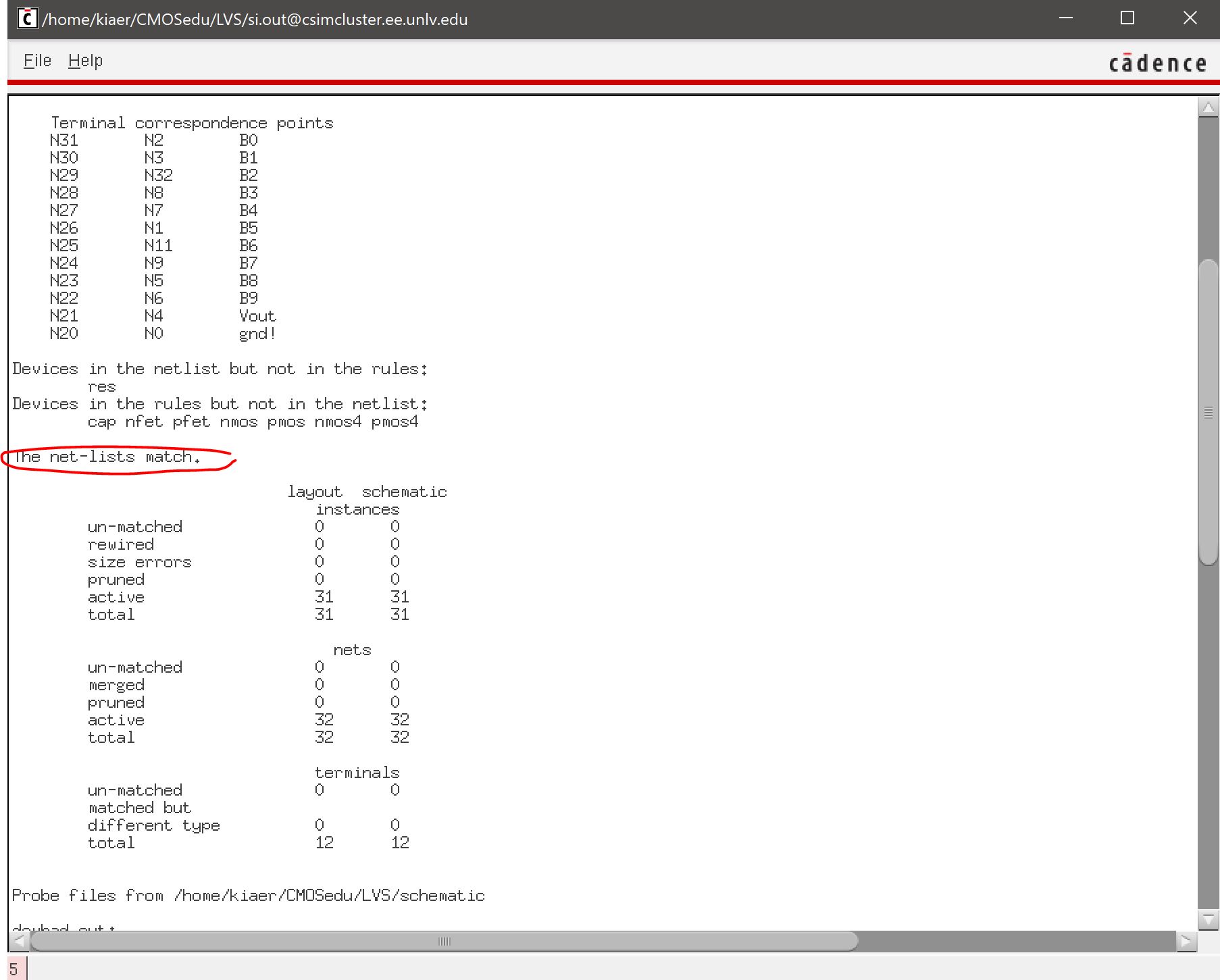
After adding the metal1 layer pins to the input, output, and gnd the next step would be to first DRC the layout to ensure there are no erros (Verify->DRC). Then to extract the layout (Verify->Extract). Then to finally LVS the extracted layout and the schematic (Verify->LVS), once doing so the output above should be the desired results. The net-lists match.


Lab description

- Use the n-well to layout a 10k resistor as discussed in Tutorial 1: 

The sheet resistance of the N-well determined by the process information from MOSIS is approximately 800 ohms per square (796 ohms/sq). This provides guidance on solving the required length of the 10K N-Well resistor. The minimum length is approximately 12 lambda which gives a minimum width of 3.6 um where lambda is 0.30 according to MOSIS. 

http://cmosedu.com/jbaker/courses/ee421L/f18/students/kiaer/lab3/snip13.JPG

- Use this n-well resistor in the layout of your DAC: 

I used a width of 4.5 um which would be over the minimum width (3.6 um) and used that as lambda. 10K/800 Ohms per square = 12.5lambda 

12.5 x 4.5 = Approximately 56 um 

I used 56.1 to be within 0.15 to fit the grid, so there are no errors when verifying DRC. 

With the measurements 4.5 um x 56.1 um I got a 10.2k resistor after extracting the layout.

http://cmosedu.com/jbaker/courses/ee421L/f18/students/kiaer/lab3/snip12.JPG

- Enesure that each resistor in the DAC is laid out in parallel having the same x-position but varying y-positions (the resistors are stacked). 

http://cmosedu.com/jbaker/courses/ee421L/f18/students/kiaer/lab3/snip14.JPG

 Here is the layout of the 10-bit DAC by using the 10K n-well layout in a stacked formation. All the 10K resistors have the same x-position but different y-positions. Each resistor is connected to another using a metal1 layer (Create->Shape->Rectangle/Path) Each pin also uses the metal1 layer. 

-All input and output Pins should be on metal 1

http://cmosedu.com/jbaker/courses/ee421L/f18/students/kiaer/lab3/snip17.JPG

The input and output pins are implemented with the metal1 layer as seen above. Also the "gnd!" pin is also used with the metal1 layer and is indicated as a inputOutput pin. Each resistor has to be at least 5.4 um apart.At first, when I DRC the first two resistors, I received an error displaying a white box in between the resistors indicating that I need to create more space between the resistors for DRC to work. 

- DRC and LVS, with the extracted layout, your design: 

http://cmosedu.com/jbaker/courses/ee421L/f18/students/kiaer/lab3/snip15.JPG

Here is the output of the DRC (Verify->DRC) of the layout I created with the stacked 10K Resistors using metal1 connections. We can see that there are no errors found. 

http://cmosedu.com/jbaker/courses/ee421L/f18/students/kiaer/lab3/snip16.JPG

Above is the output of the LVS displaying that the net-lists match using the layout of my design (extracted) vs the schematic I created in Lab 2 of the 10-bit Ideal Digital to Analog Converter.

Here is the .zip file of the Lab3 Design directory with the layout, schematic, and Lab 2 files: Lab 3

Return