EE 421 Lab (Digital Integrated Circuit) - Fall 2018
11/14/18
Project
Requirements:
Design a serial to
parallel converter that takes serial input data and an associated clock signal and
generates an 8-bit output (parallel) word and clock.
The circuit inputs
are Din and clk_in.
The circuit outputs
are D0-D7 and clk_out.
If the serial input
is 10 Mbits/s then the parallel output is 1.25 MWords/s.
Your serial-parallel
design should show various inputs to verify it works.
First
Half of the Project: Schematic with several sample simulations
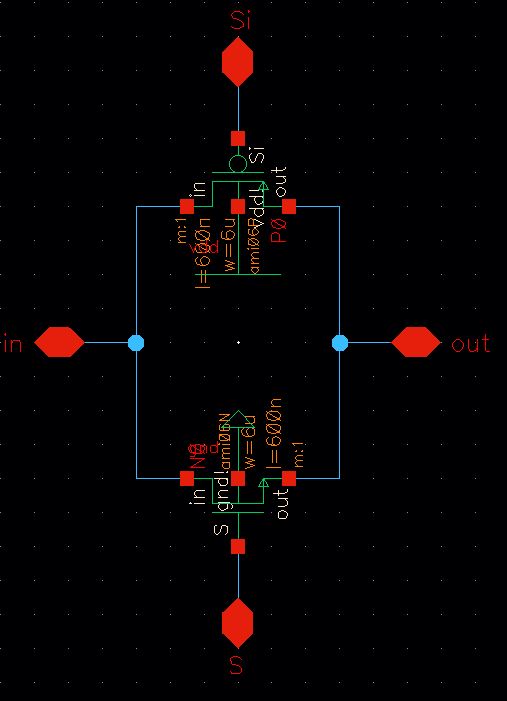
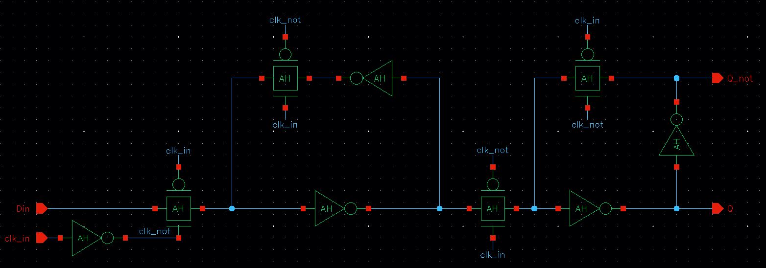
-In order to design a schematic
for a serial to parallel converter, Transmission Gates (TG), inverters, and D
Flip-Flops (D-FF) are created.
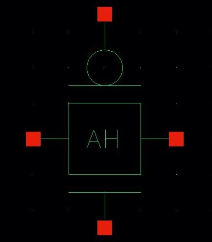
o
Symbol
·
Inverter:
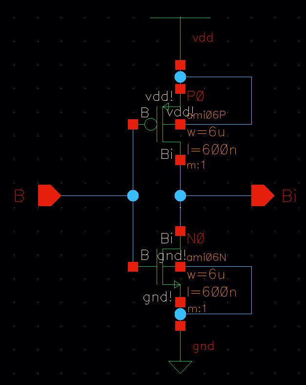
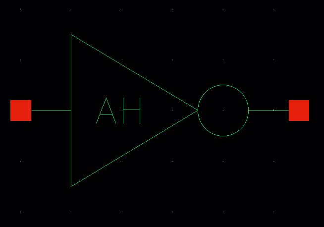
o
Symbol
·
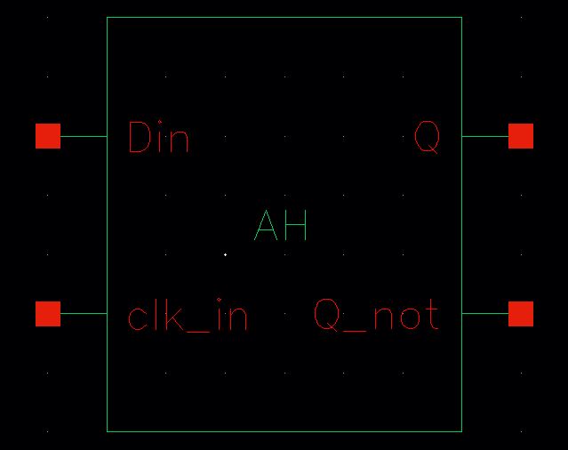
D Flip-Flops (D-FF):
o
Symbol
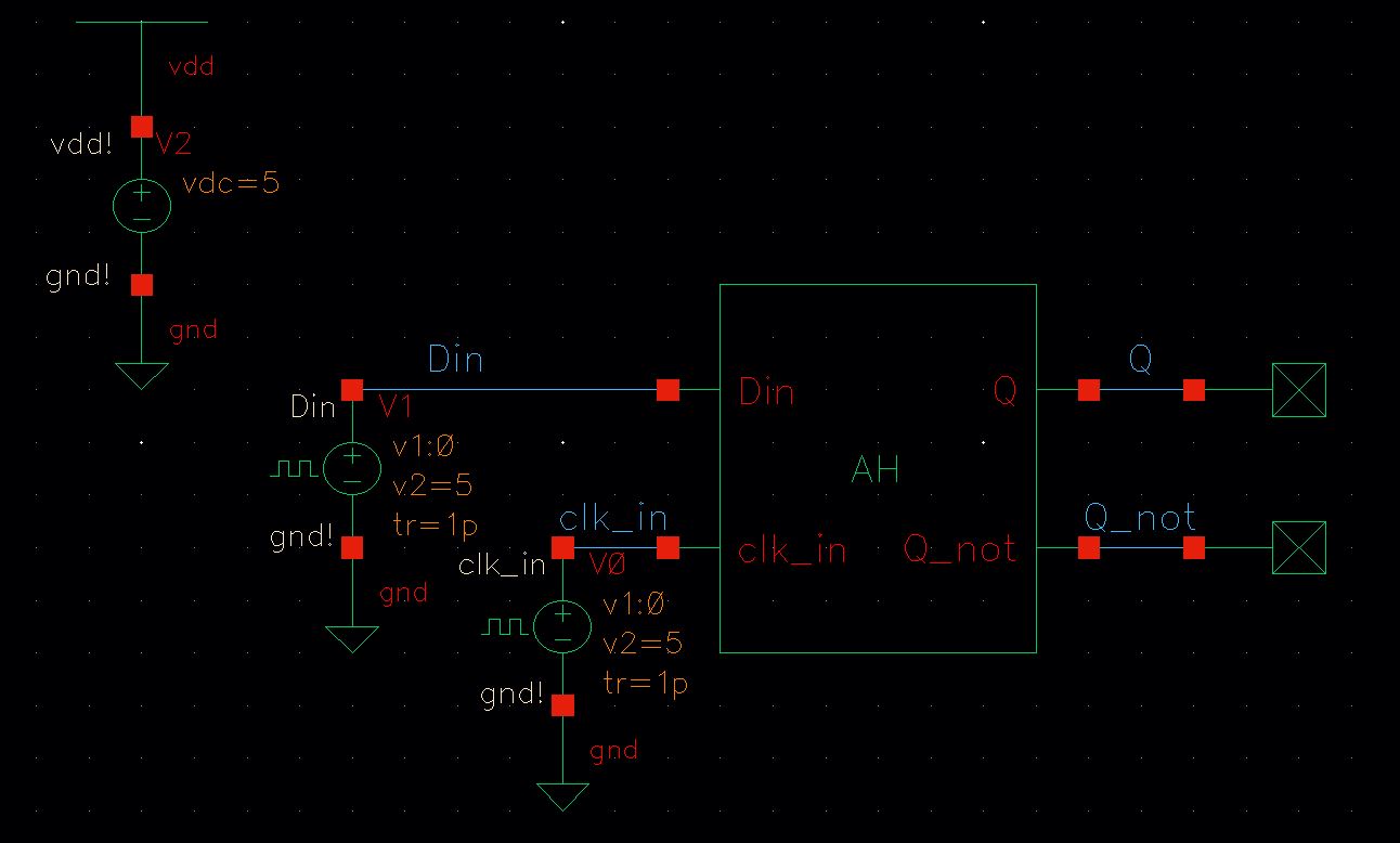
o
Schematic to simulate D-FF
o Simulation result
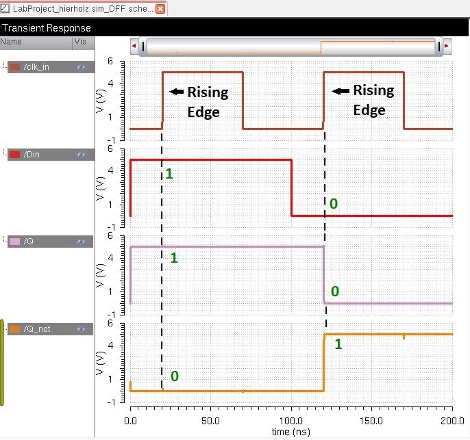
At the rising edge of the clock, Q saves the input of Din and it remains the same until the next rising edge of the clock.
Clk_in has a 20ns delay. Right when clk_in goes high, Din is high so Q stay high until the next rising edge.
At the next rising edge, Din is low, so Q goes low and stays low until the next rising edge.
Q_not then does the opposite of Q.
o
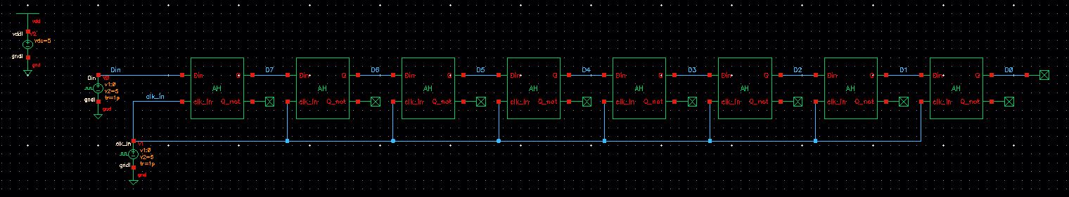
Schematic to simulate shift register
o
Simulation Result
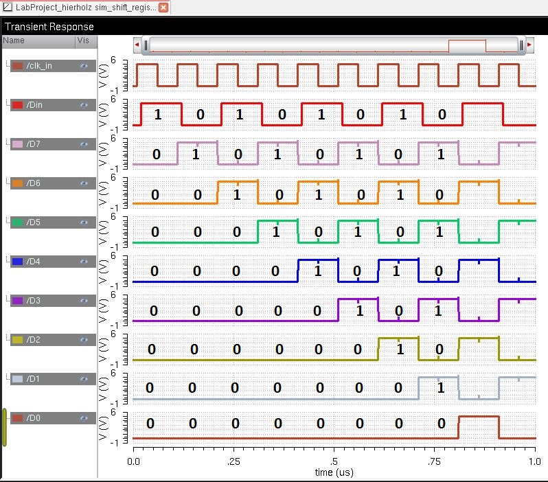
When clk_in goes high, Din
goes through each flipflop and keeps shifting until it reaches the 8th bit
·
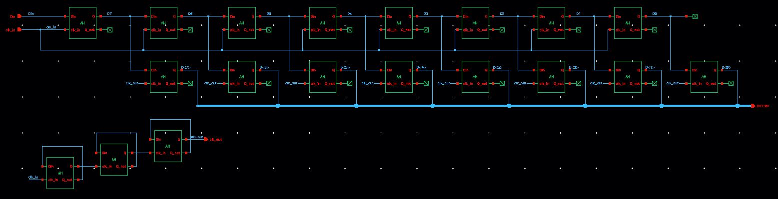
Another set of 8 D-FF in series are connected in parallel to the
first set of 8 D-FF to create an 8-bit serial to parallel converter
o
If the serial input is 10 Mbits/s clk_in has a frequency of 10MHz
in order to grab each bit; so, clk_in/8 reduces the frequency of the input clk
by 8 times.
o
If the period of clk_in is T = 1/f = 100ns, the period of clk_in/8
should be 8 times that which is 800ns.
o
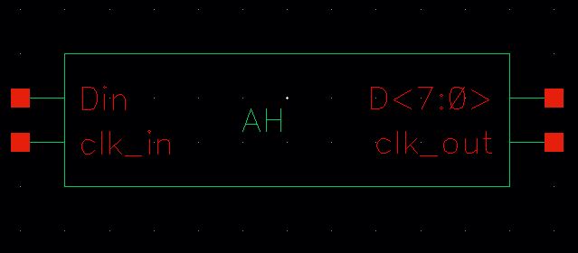
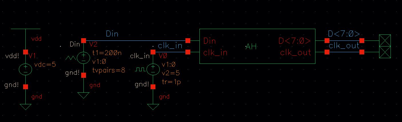
Schematic for serial to parallel converter
o
Symbol
o
Schematic to simulate serial to parallel converter
o
Simulation result
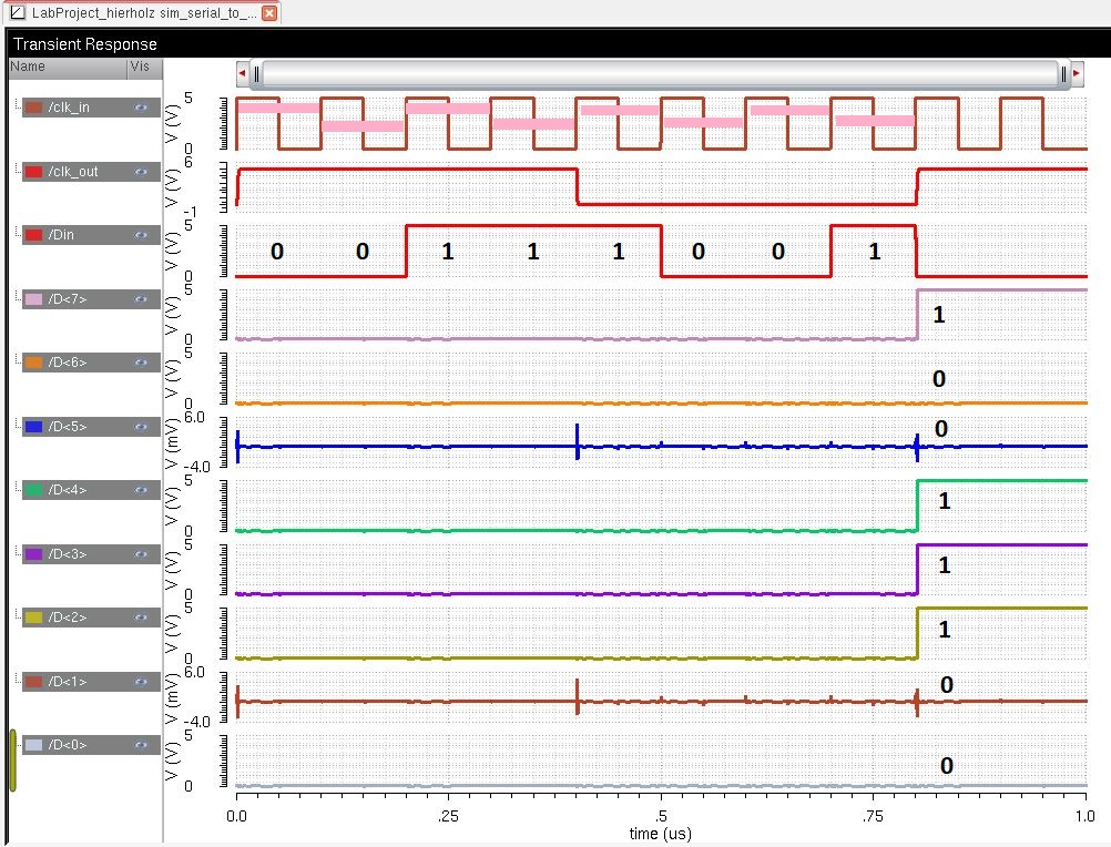
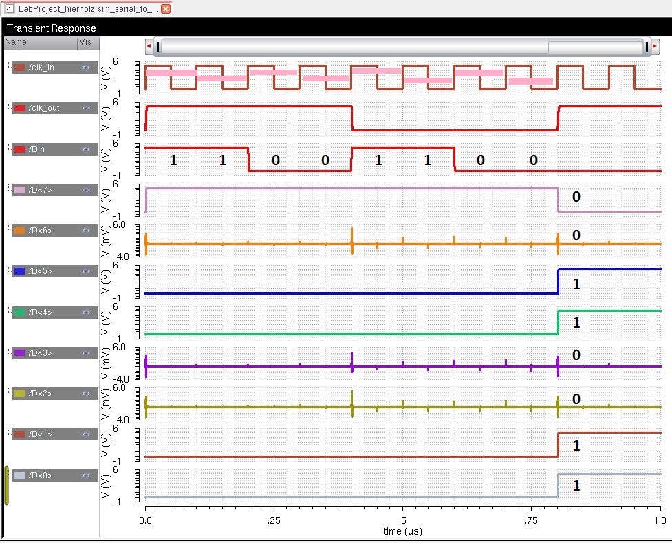
The input used for this
simulation is Din = 10011100. PieceWiseLinear Voltage source was used to create
this input.
Clk_in has a period of 100ns,
so in order to grab each bit of the input, the pulse width of each bit should
100ns, with a period of 200ns.
The least significant bit is
the first input and it keeps shifting until it reached the 8th bit.
Once 8 bits are saved, clk_out
goes high and outputs D7=1, D6=0, D5=0, D4=1, D3=1, D2=1, D1=0, D0=0.
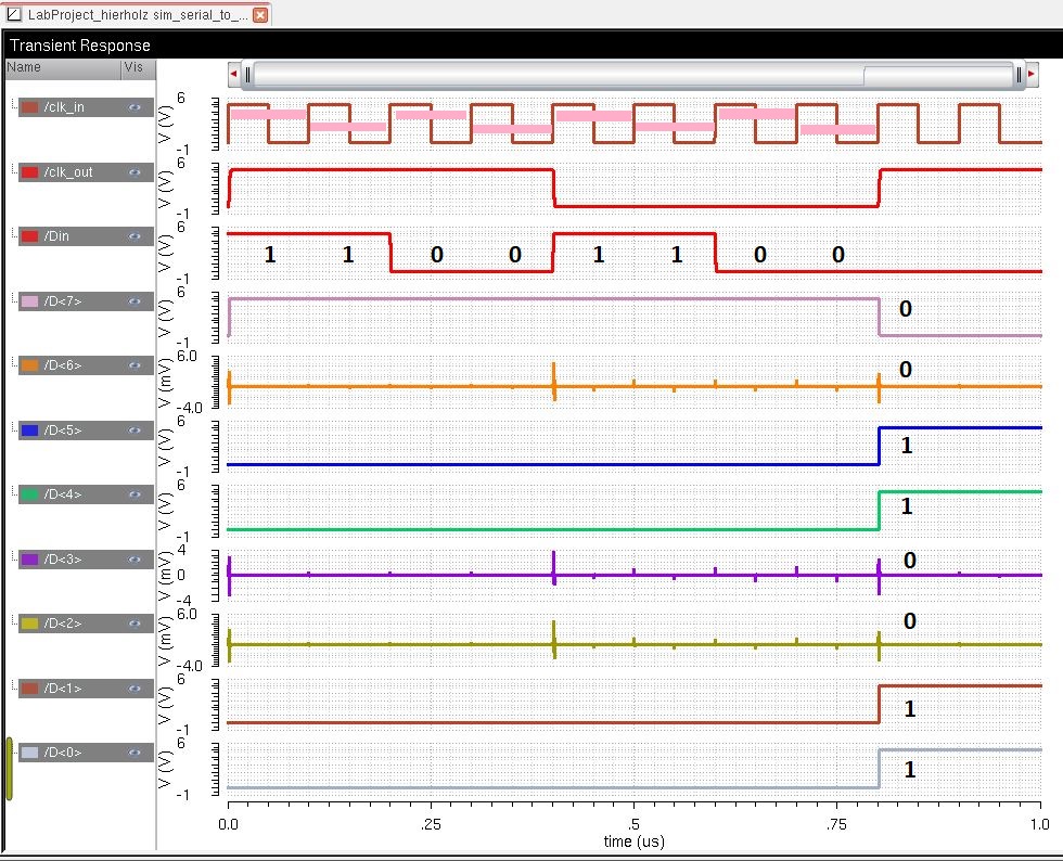
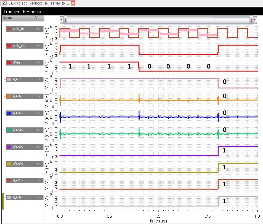
Extracted simulation: Extracted view is
used to test that the layout is working properly. In this simulation,
the inputs from Ex2 was chosen to compare with the
extracted view simulation. The results in Ex2 should match the result in extracted view simulation.
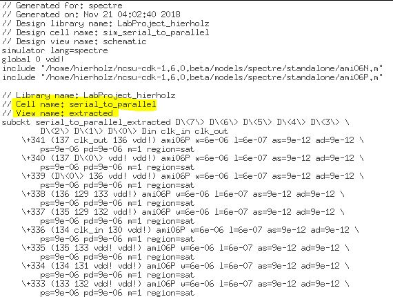
Result:
Second Half of the Project: A verified layout and documentation
-D-FF· Layout
· Extracted
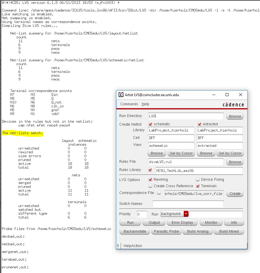
· LVS
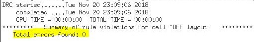
· DRC
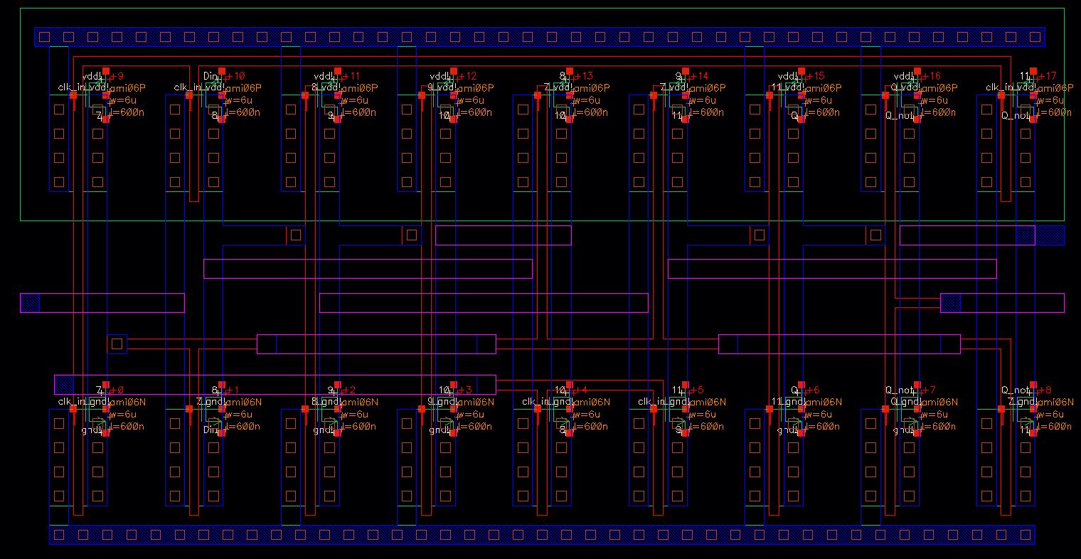
-Serial To Parallel Converter
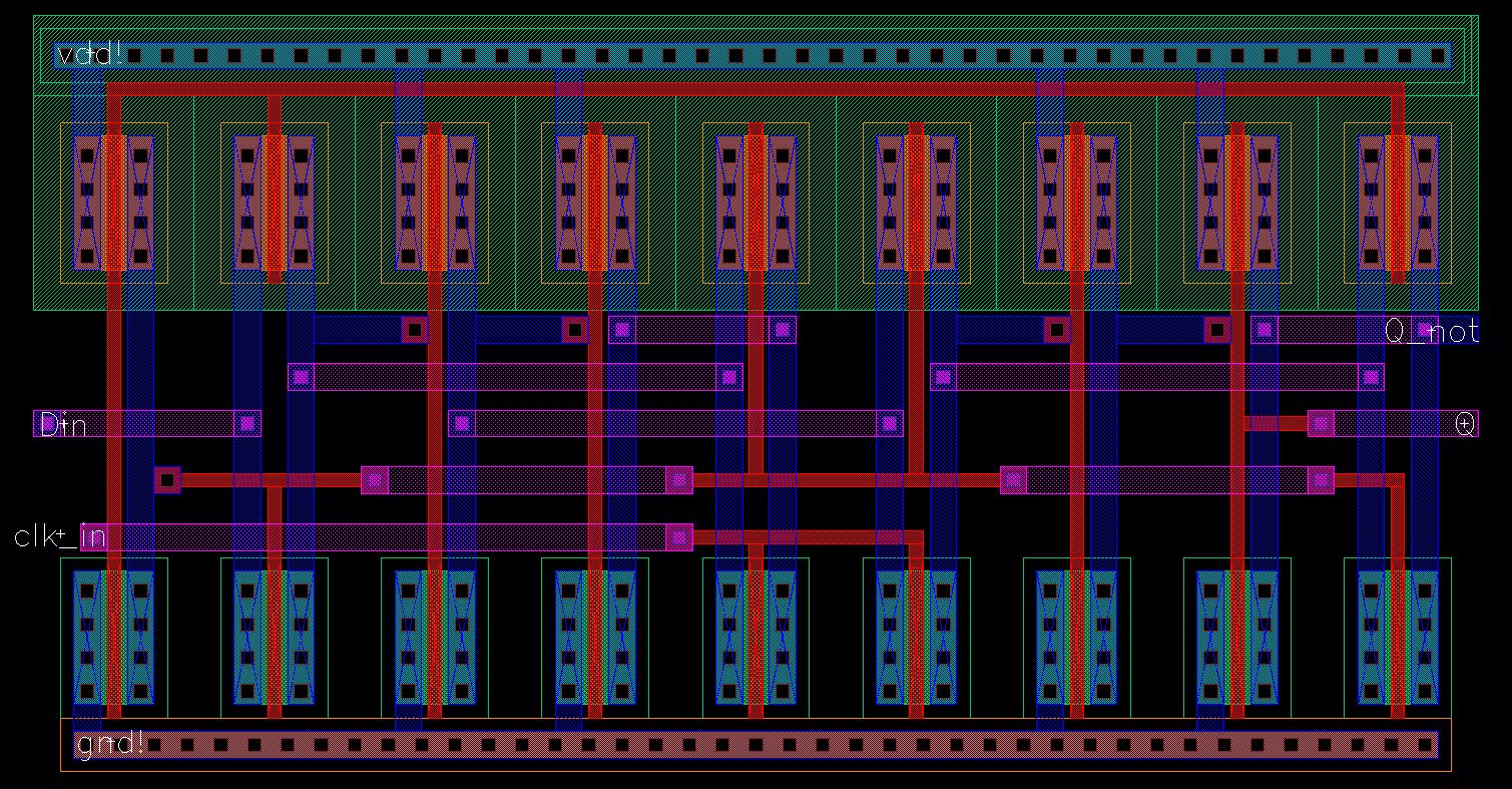
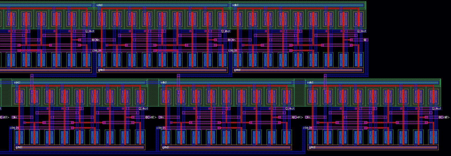
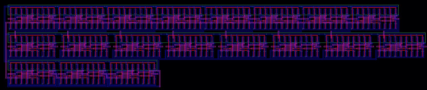
· Layout
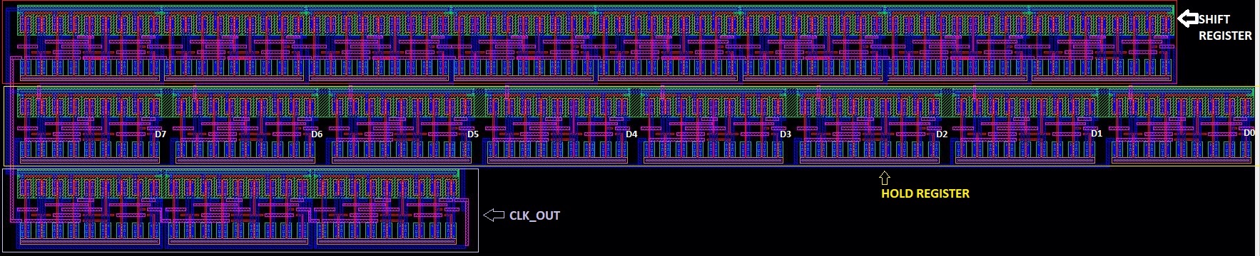
· Segments of layout for a closer view
(1) D<5> on the right side is connected to D<5> on the left side of the (2) second segment 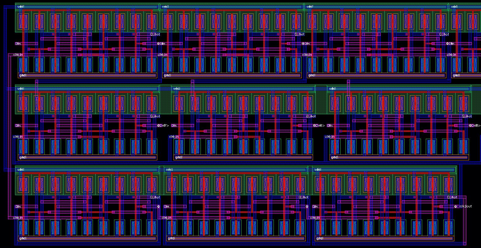
(2) D<3> on the right side is connected to D<3> on the left side of the (3) third segment
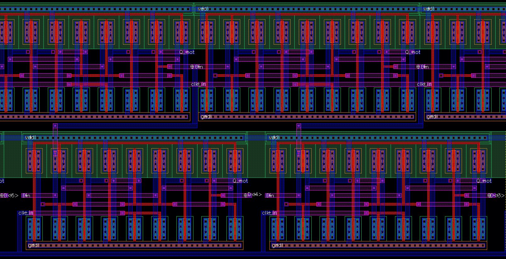
(3)
· Extracted
·
LVS: To compare the schematic and layout using the extracted view and make sure all net lists match
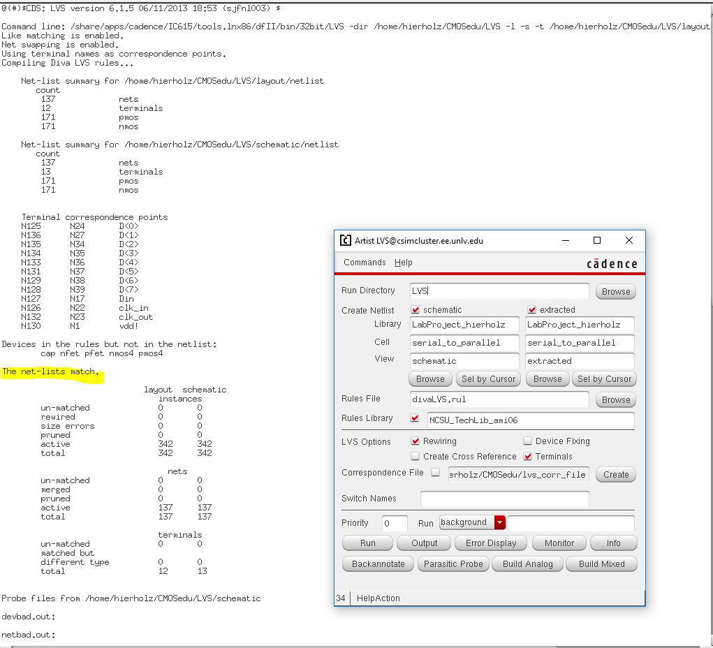
·
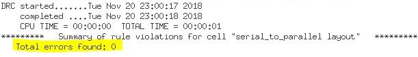
DRC: To make sure that there are no violations on the layout
The cells used to generate the images used on this webpage can be downloaded in
proj_hie
Return
to EE 421 Lab
Return
to Student Lab Reports