Lab 8 - EE 421L - Digital Integrated Circuit Design
Generate a test chip layout for submission to MOSIS for fabrication
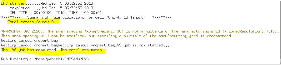
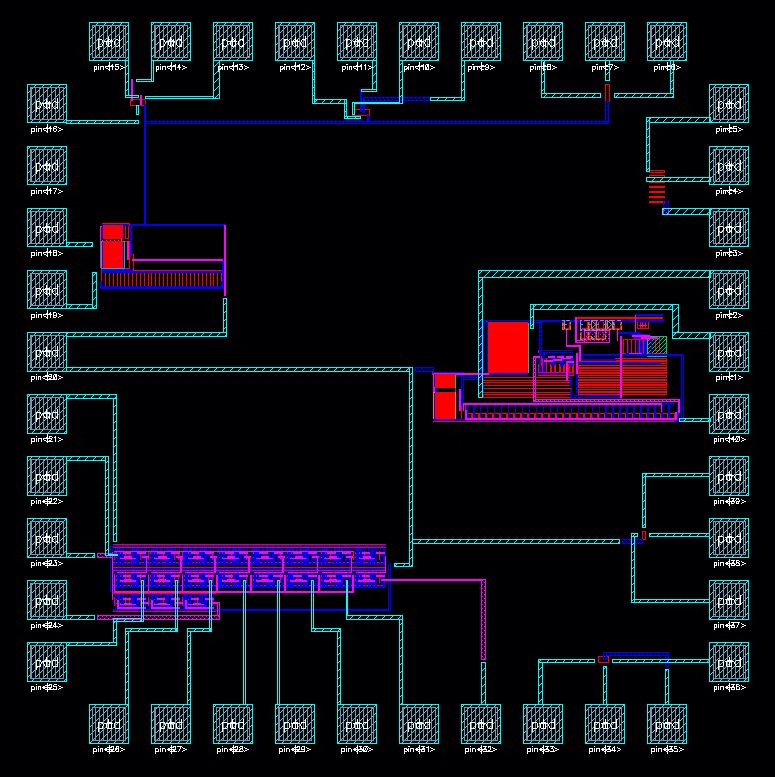
Link to Directory: Chip4_f18
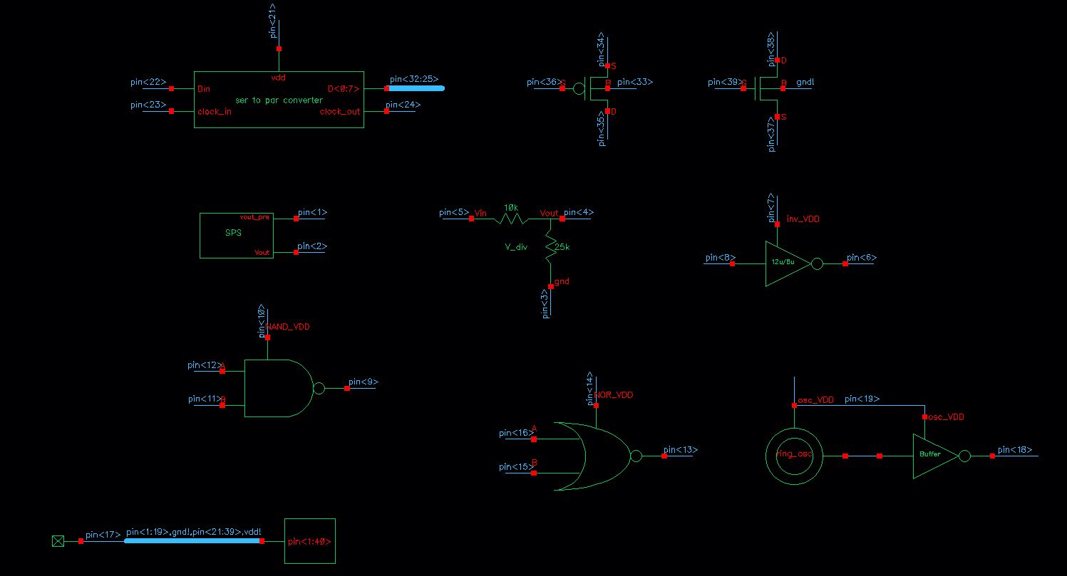
| Chip Schematic | Chip Layout |
| |
| Symbol | How to test |
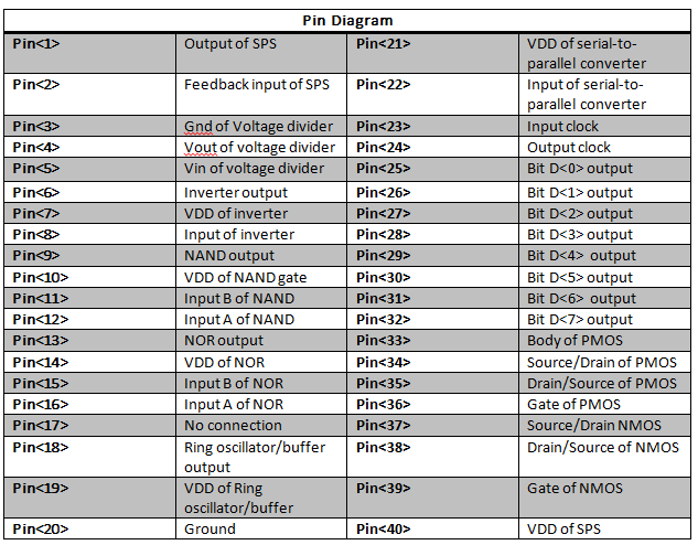
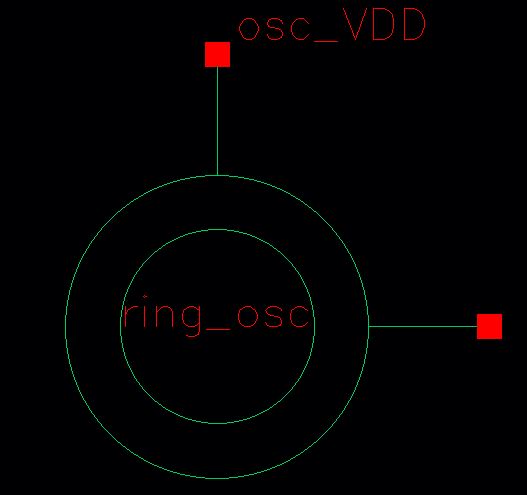 | Ground pin<20> Connect 5V VDD to pin<19> Measure the output at pin<18> |
| Symbol | How to test |
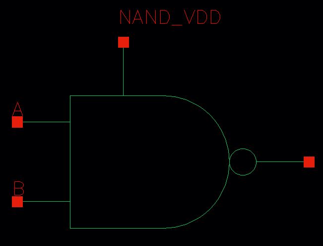 | Ground pin<20> Connect 5V VDD to pin<10> Apply inputs to pin<11> and pin<12> Measure the output at pin<9> |
| Symbol | How to test |
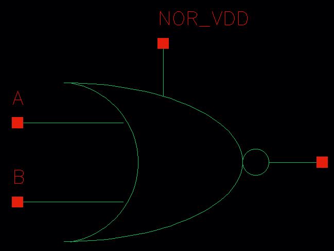 | Ground pin<20> Connect 5V VDD to pin<14> Apply inputs to pin<15> and pin<16> Measure the output at pin<13> |
| Symbol | How to test |
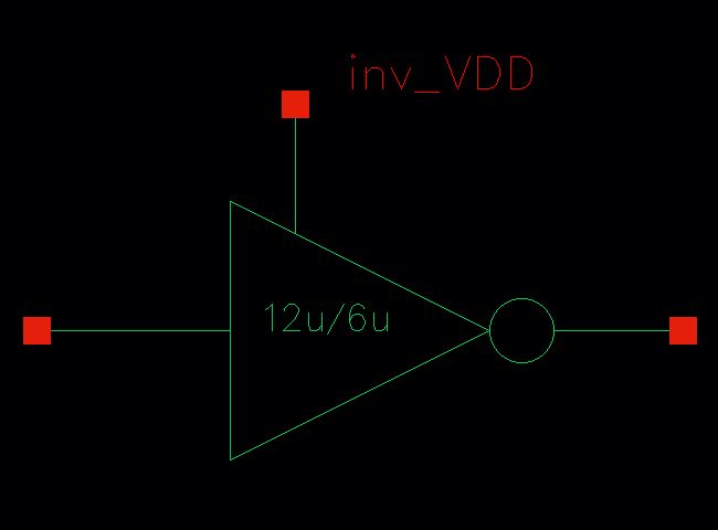 | Ground pin<20> Connect 5V VDD to pin<7> Apply input to pin<8> Measure the output at pin<6> |
| Symbol | How to test |
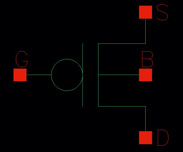 | Apply 5V VDD to body at pin<33> Drain connection at pin<35> Source connection at pin<34> Gate input at pin<36> |
| Symbol | How to test |
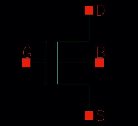 | Ground the body at pin<20> Drain connection at pin<38> Source connection at pin<37> Gate input at pin<390--> |
| Symbol | How to test |
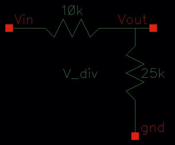 | Ground pin<3> Apply Vin at pin<5> Measure Vout at pin<4> |
| Symbol | How to test |
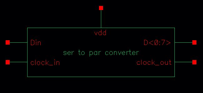 | Ground pin<20> Apply 5V VDD to body at pin<21> Apply input to pin<22> Apply input clock to pin<23> Measure the output at pin<25:32>, these are parallel output of the system Measure the clock out at pin<24>, |
| Symbol | How to test |
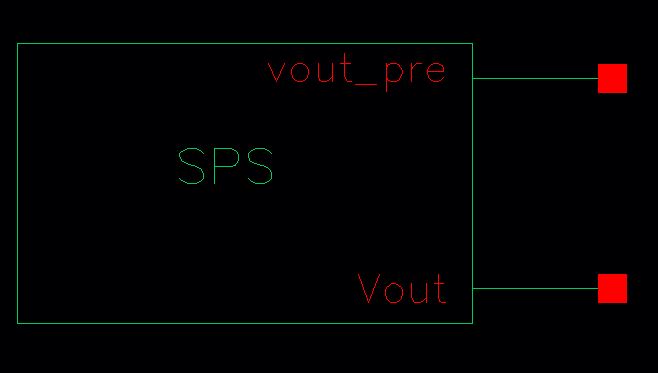 | Ground pin<20> Measure the output of SPS at pin<1> This pin connects to a 30uH inductor and to a schottky diode. The inductor is connected to VDD on the other side. The other side of the diode is connected to a 5uF capacitor and load resistor of 250 Ohm. The node connected to the capacitor and load resistor is Vout and is used as the feedback into the system of the SPS. This ciruict composes a Boost SPS. Measure the feedback inpu at pin<2> which is labeled Vout |