Lab 4 - EE 421L
Allis Hierholzer
hierholz@unlv.nevada.edu
9/26/18
Pre-Lab:
- Back-up all work from the lab and the course
- Read
through the lab instructions prior to starting the lab
- Finish
Tutorial 2
Lab Description:
- This lab focuses on IV
characteristics and layout of NMOS and PMOS devices in ON's C5 process.
- First, generate schematics
and simulations for NMOS and PMOS devices.
- ID
v. VDS of an NMOS device for VGS varying from 0 to 5 V in 1 V steps while VDS
varies from 0 to 5 V in 1 mV steps. Use a 6u/600n width-to-length ratio.


- ID
v. VGS of an NMOS device for VDS = 100 mV where VGS varies from 0 to 2 V in 1
mV steps. Again use a 6u/600n width-to-length ratio.


- ID
v. VSD (note VSD not VDS) of a PMOS device for VSG (not VGS) varying from 0 to
5 V in 1 V steps while VSD varies from 0 to 5 V in 1 mV steps. Use a
12u/600n width-to-length ratio.


- ID
v. VSG of a PMOS device for VSD = 100 mV where VSG varies from 0 to 2 V in 1 mV
steps. Again, use a 12u/600n width-to-length ratio.


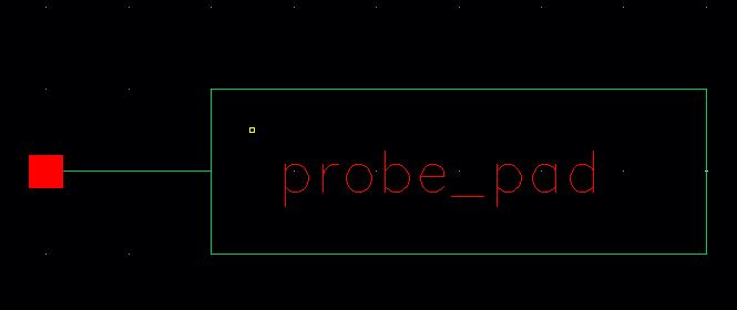
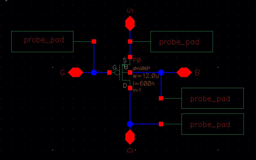
- Create
a layout for each devices and connect all 4 MOSFET terminals to probe pads. Show
that each layout passes DRC, then LVS each layout.

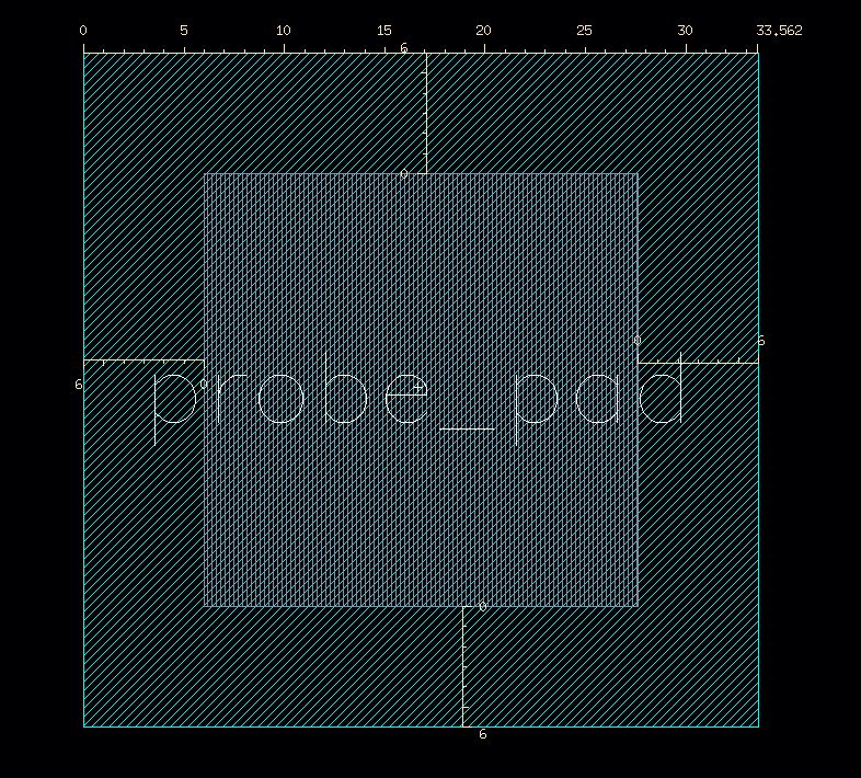
- Create a 6u/0.6u NMOS device

- Layout of NMOS device along with the zoomed in connections of all 4 MOSFET terminals to the probe pads


- The layout passed DRC and LVS was performed


-
Create a 12u/0.6u PMOS device
- Layout of PMOS device along with the zoomed in connections of all 4 MOSFET terminals to the probe pads
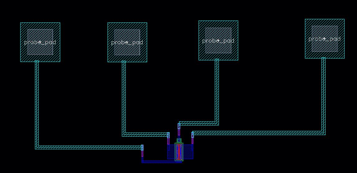

- The layout passed DRC and LVS was performed


The cells used to generate the images used on this webpage can be downloaded in Lab4_hie
Return to EE 421 Lab
Return to Student Lab Reports