Lab 2 - EE 421L
-Upload the ideal 10-bit Analog-to-Digital Converter (ADC) and Digital-to-Analog Converter(DAC) simulation example in design directory CMOSedu
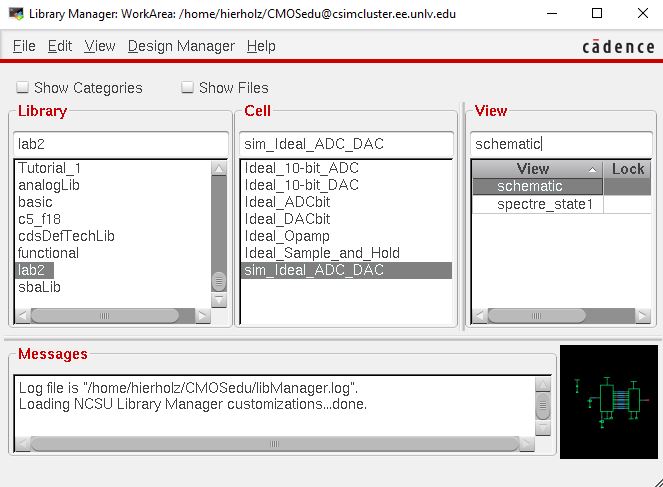
-Open the schematic view of the cell sim_Ideal_ADC_DAC
-Run the simulation (Plot can be edited by right clicking on the graph and selecting "graph properties." )
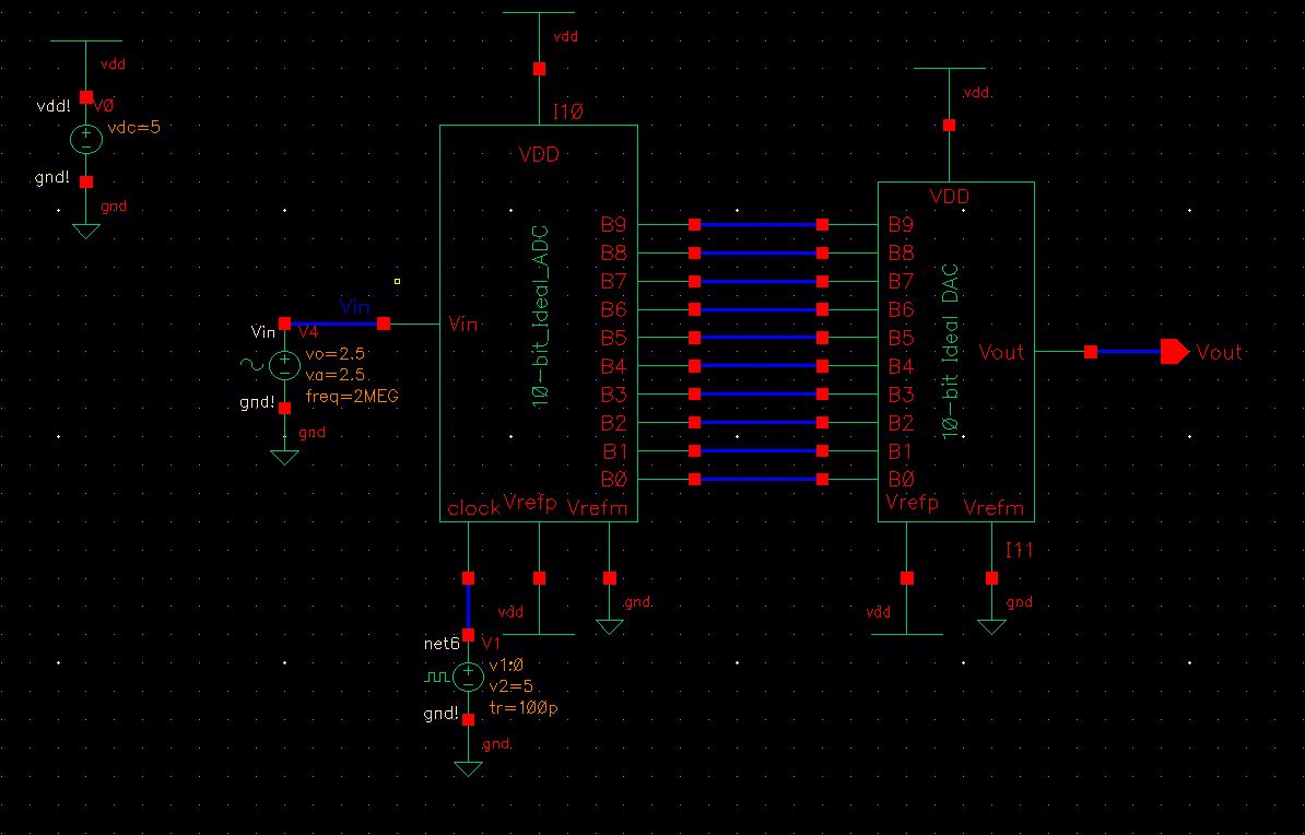
-Understand how the input voltage (Vin) is related to B[9:0] and Vout:
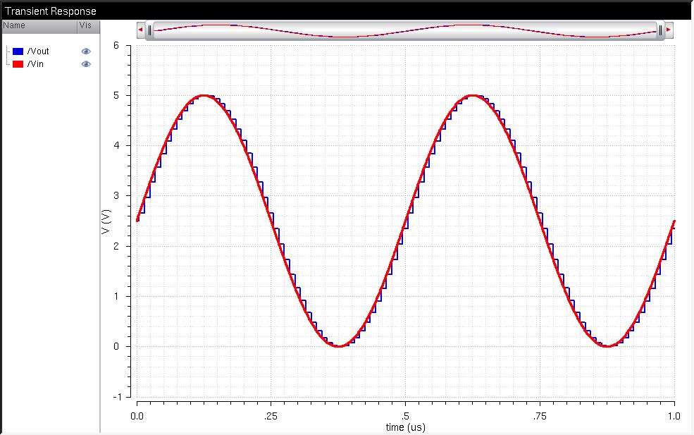
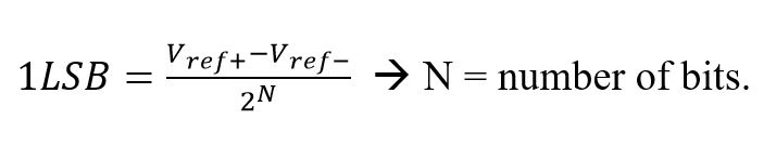
Suppose a 10-bit DAC uses 5V and ground for reference voltages; using the formula shown below, 1LSB = 4.9mV. Vout would follow Vin at the rate of 4.9mV per step.
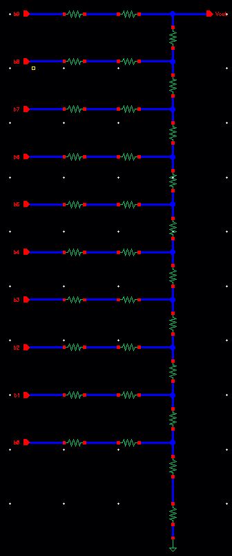
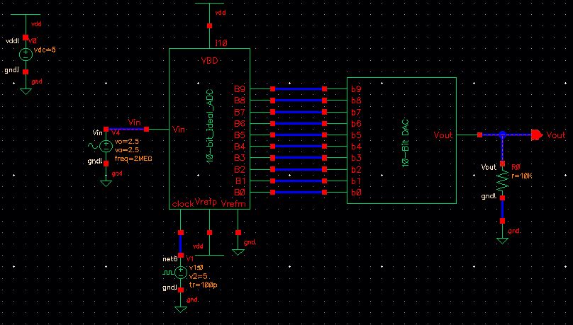
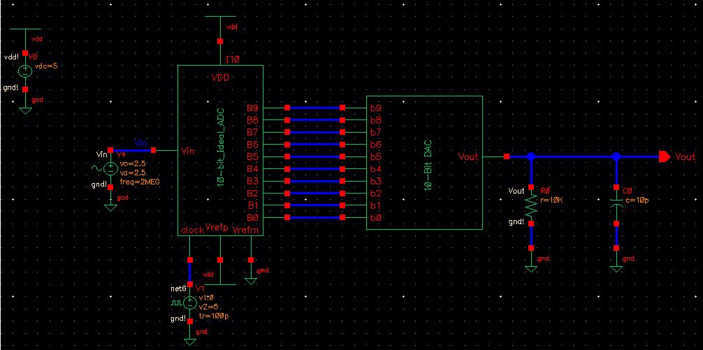
-In this lab, n-well resistors are used to implement a
10-bit DAC based on Figure 30.14 (shown below).
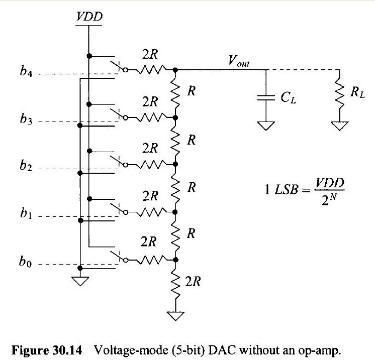
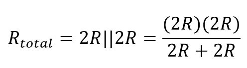
-To design a 10-bit DAC, the resistors should be implemented by having two 10k resistors in series that is parallel to a one 10k resistor, per bit.
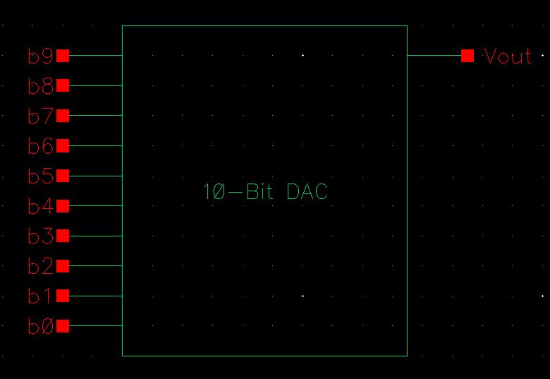
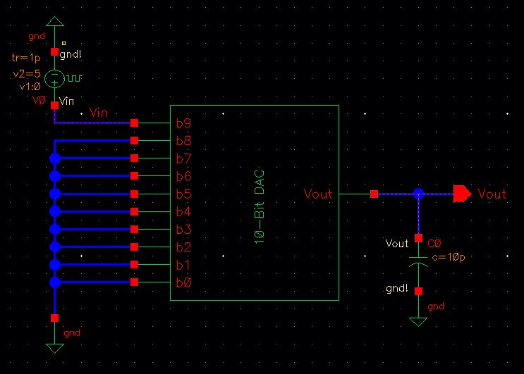
-Create a symbol for the 10-bit DAC design:
~On the tabs on the schematic
window, click on "Create" -> "Cellview" -> "From Cellview" ->
"ok"
~Label the left pins b9-b0, the right pin Vout
-The 10-Bit DAC total resistance is equal to 10k
-The delay when driving a 10pF load is 70ns
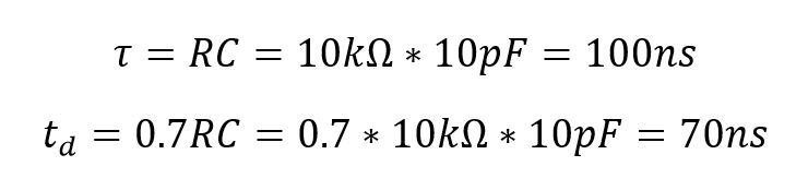
-The DAC is behaving like a voltage divider, where Vout becomes half of Vin after 5RC
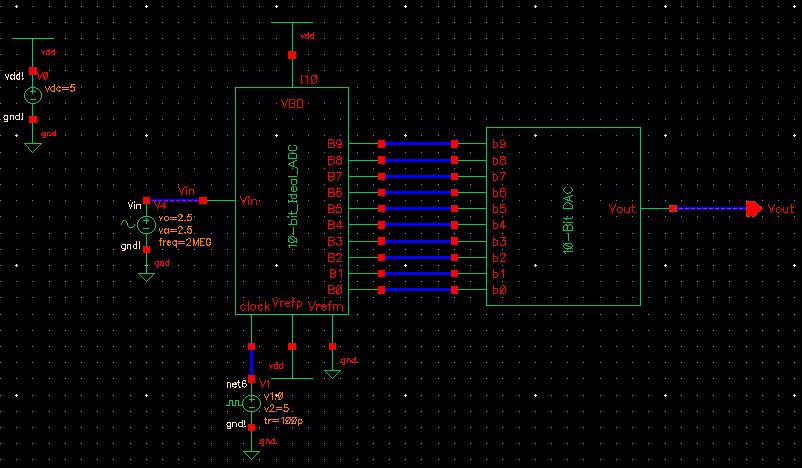
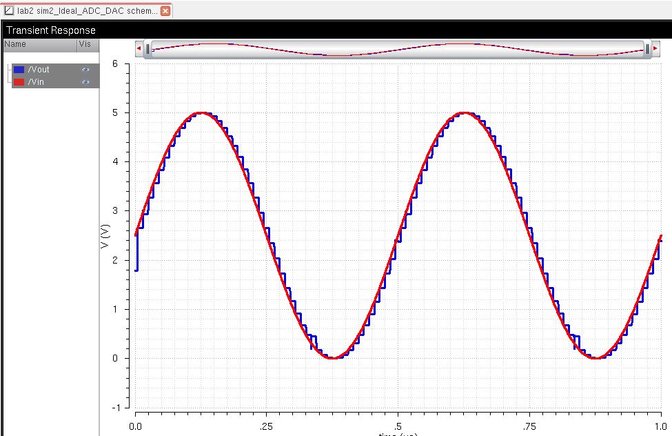
-ADC connected to the created DAC with no load
-DAC under no load: Vout waveform is the same waveform as Vin
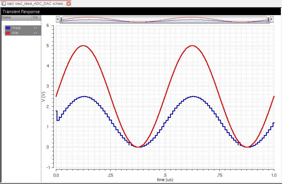
-ADC connected to the created DAC with resistive load of 10k
-DAC with resistive load: the waveform of Vout is half as much Vin
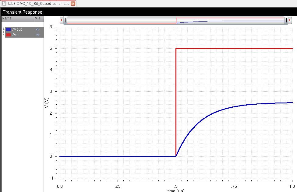
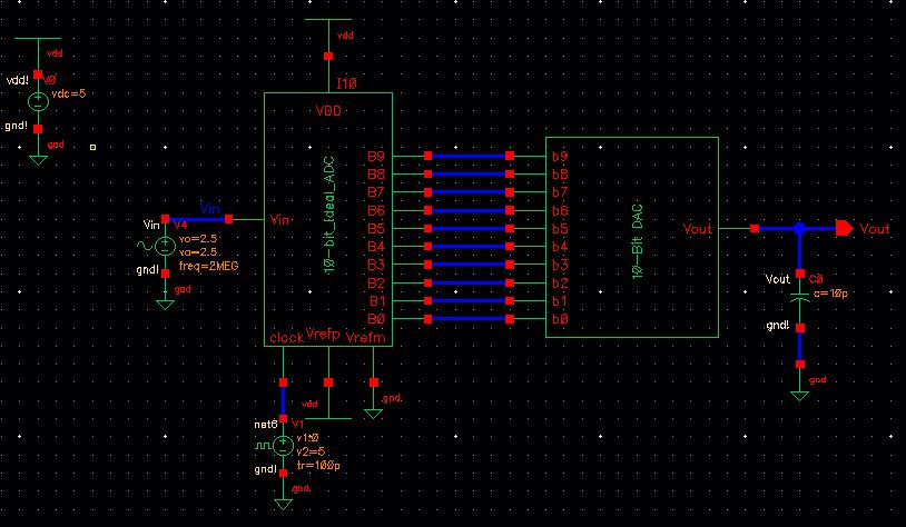
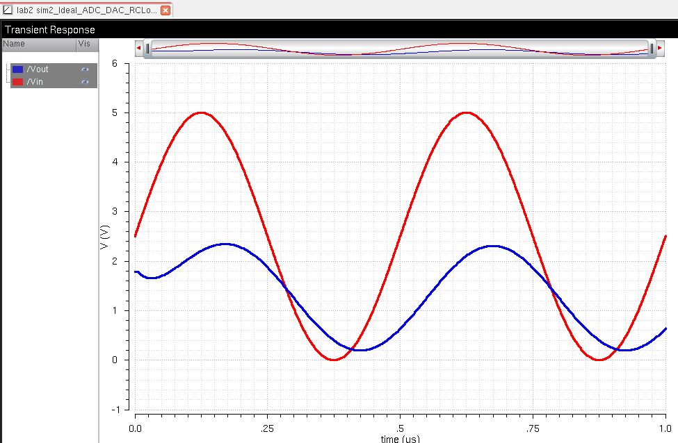
-ADC connected to the created DAC with capacitive load of 10pF
 http://cmosedu.com/jbaker/courses/ee421L/f18/students/hierholz/Lab2/Photos/10_RCLoad_Sim.JPG
-DAC with capacitive load creates a DC offset of 1V on Vout
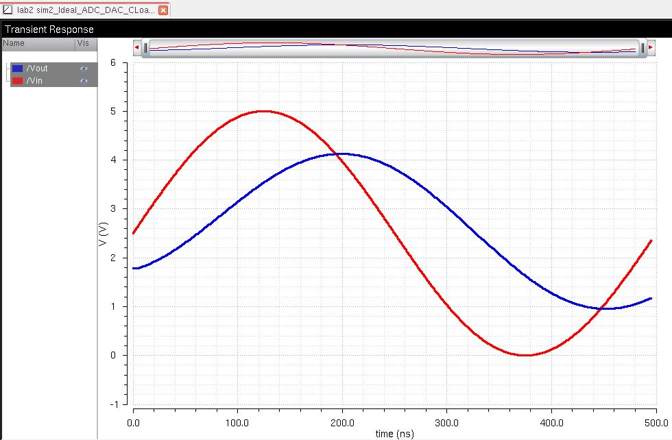
-ADC connected to the created DAC with both capacitive load of 10pF & resistive load of 10k
-DAC with both capacitive load of 10pF &
resistive load of 10k shows a big decrease in voltage between Vin andVout
The cells used to generate the images used on this webpage can be downloaded in Lab2_hie