Lab 1 - EE 421L
Allis Hierholzer
Email: hierholz@unlv.nevada.edu
9/5/2018
Prelab
The prelab required getting a
CMOSedu account from Dr. Baker and review webpage editing. A student should be
able to perform file transfers from the desktop to the website such as
documents, folders, images, etc.
Lab Description
This lab introduces webpage editing
and Cadence for chip design, layout, and simulation. The first part of the lab
required the installation process of Cadence along with several files needed to
be added to the library so that Cadence run properly; several examples from the
book are also added to the library for a much faster simulation result. At the
end of every lab, students should always download a zipped file of their work
and upload it to google drive for back up purposes.
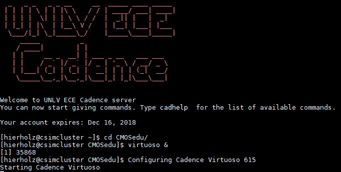
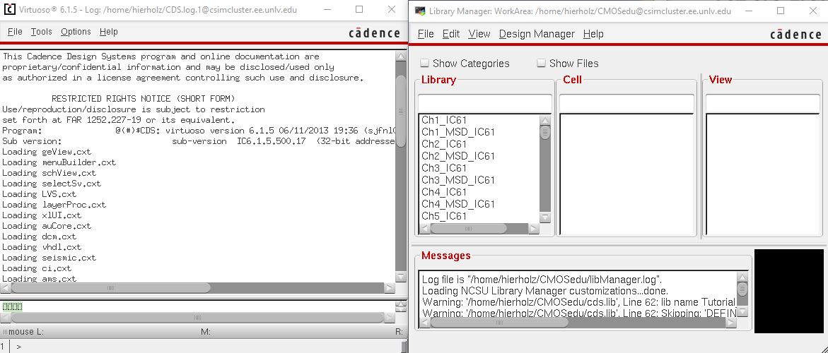
Once Cadence is installed, run the
program using the command “Virtuoso &”.

(Two windows should appear: Command Interpreter & Library
Manager).
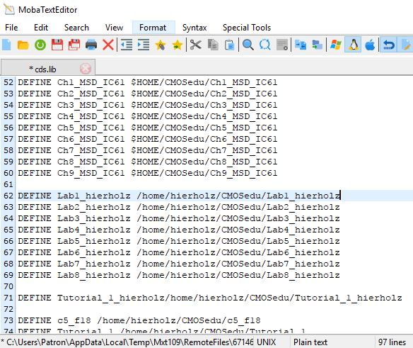
Next, create a library; when a library is created, a definition line is added to the cds.lib file.
For example, I created a library for Lab 1-6 named it Lab1_hierholz, Lab2_hierholz, and so on.
The remaining part of the lab is
becoming familiar with Cadence and being able to demonstrate its operations.
- First, we will be simulating a simple voltage divider
- Create a schematic by instantiating (using bindkey "i") a
voltage source, two resistors, and ground (these components can be
found under the library "NCSU_Analog_Parts")
- To edit the values/properties of each components, use bindkey "q"
- Connect these components using bindkey "w" for wiring
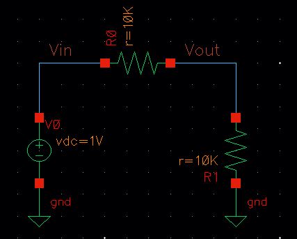
- Check and save and look at the command window to make sure no errors are found

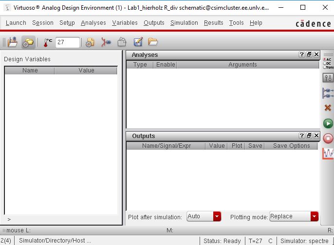
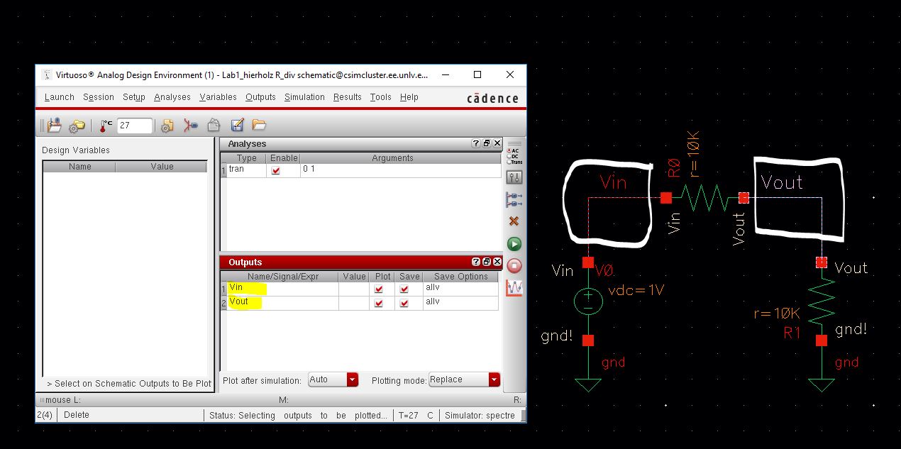
- Run the simulation by clicking "Launch" > "ADE L" and your Analog Design Environment window should open up

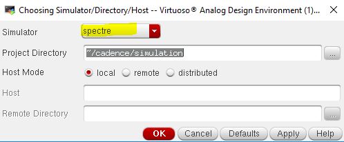
- We'll assume throughout this tutorials that
Spectre is used as simulator; to verify, Click "Setup" >
"Simulator/Directory/Host ..."

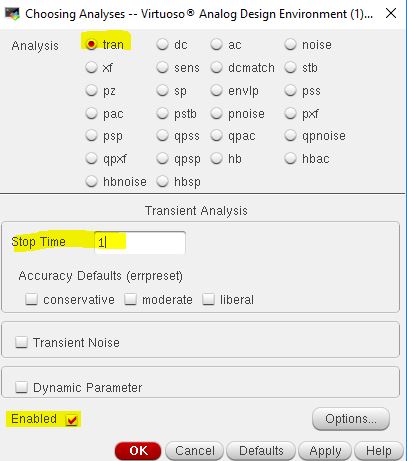
- Now,
perform a transient analysis with a Stop Time of 1s by clicking
"Analyses" > "Choose" > "tran" and also select "Enabled" at the
bottom of the window and press "ok"

- To select outputs to plot on the schematic, select "Outputs" > "To Be Plotted" > "Select On Schematic"
- Go to your schematic window and select the wire for Vin and Vout to plot the input and output voltage
- Those wires you selected should turn into dash lines and should also appear on your ADE window under "Outputs"

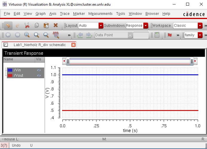
- Click the green button on the right on your ADE window to run the simulations
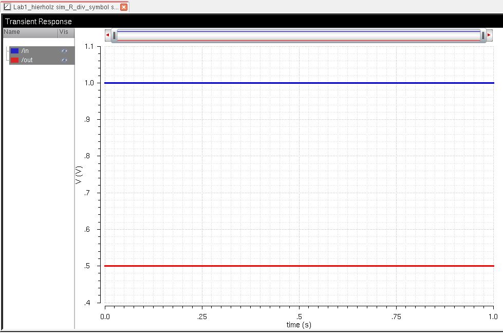
- Vout (0.5V) should be half of Vin (1V)

- Saving simulation results:
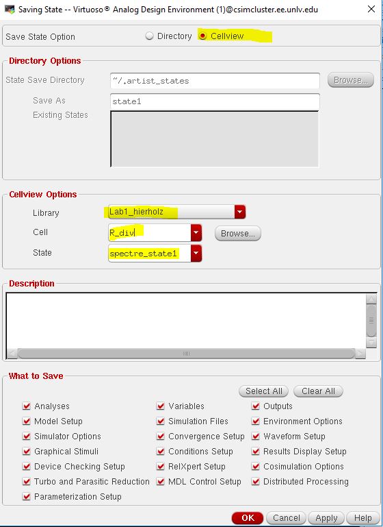
- Go back to ADE window. Under "Session", click "Save State" and a Saving State window should come up
- Select "Cellview" and double check that you are in the correct Library and click "ok"

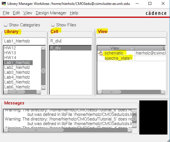
- You may
close the ADE window and go to your Library Manager to check that under
View, you have a "schematic" and "a spectre_state1"

- Now, we will be creating a symbol for our voltage divider schematic
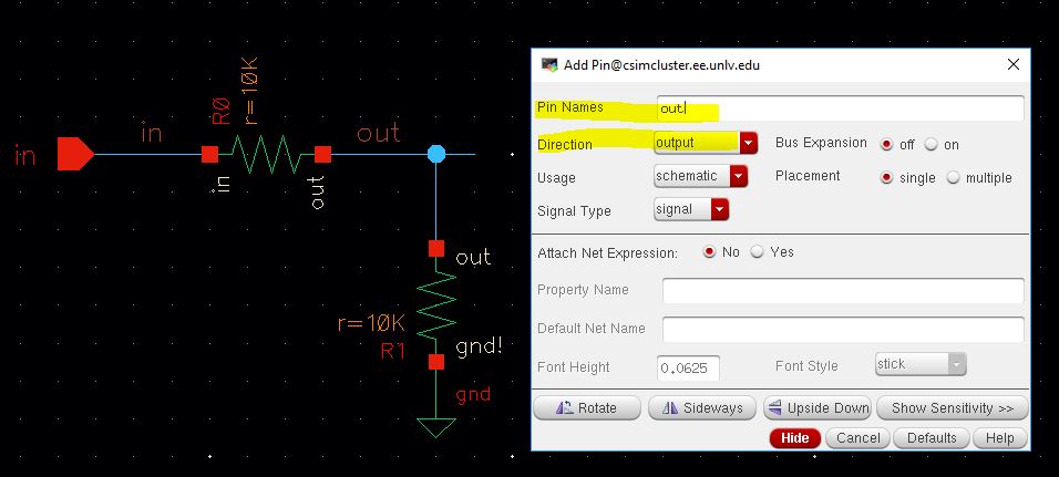
- Remove the voltage source and extend the wire of Vout
- Also, change the label of the wire Vin to in and Vout to out
- Use bindkey "p" to create a pin
- Name the input pin in and the output pin out
- Make sure
that if you're creating an input pin, you select input under "Direction"
and same with the output, select output under "Direction"
- Now, go to "Create" > "Cellview" > "From Cellview"
- Double
check the informations if it's correct and make sure that under
"Tool/Data Type", you selected "schematicSymbol" then press "ok"
- Another window should appear and double check the informations given, and press "ok"
- The next window to appear is your symbol

- As long as you leave the pins, you can modify the look of your symbol
- Click on "Create" > "Shape"
- Under "Shape", you have options to draw however you want your symbol to look like
- In my symbol, I used lines to create two resistors to represent my Voltage Divider Symbol

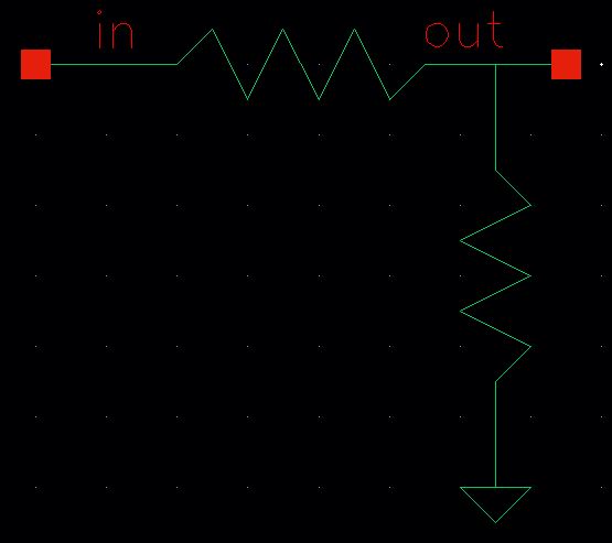
- To simulate the symbol, copy R_div cell to the same library
- I renamed
it "sim_R_div_symbol" also, make sure to select "Update Instances"Open
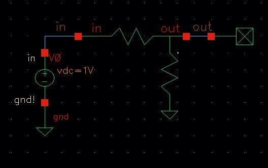
schematic and delete everything, then instantiate a voltage source
- Instantiate your symbol by selecting the library you save your symbol from.
- Complete the circuit and simulate using ADE L again, the results should be the same as the one obtained earlier
The cells used to generate the images used on this webpage can be downloaded in Lab1_hie
Return to EE 421 Lab
Return to Student Lab Reports
