Lab 8 - EE 421L - Digital Integrated Circuit Design

Generate a test chip layout for submission to MOSIS for fabrication 
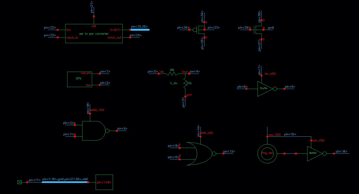
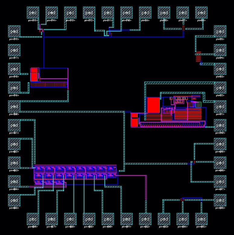

Authors:

Allis Hierholzer: hierholz@unlv.nevada.edu

Francisco Mata Carlos: matacarl@unlv.nevada.edu

Biruk Gebremeskel: gebreb1@unlv.nevada.edu


12/5/18


Pre-Lab:


Lab Description:

 Generating a test chip layout for submission to MOSIS for fabrication:
Chip SchematicChip Layout
http://cmosedu.com/jbaker/courses/ee421L/f18/students/gebreb1/lab8/final_schem.JPGhttp://cmosedu.com/jbaker/courses/ee421L/f18/students/gebreb1/lab8/final_layout.JPG
SymbolHow to test
http://cmosedu.com/jbaker/courses/ee421L/f18/students/gebreb1/lab8/ring_osc_sym.JPG
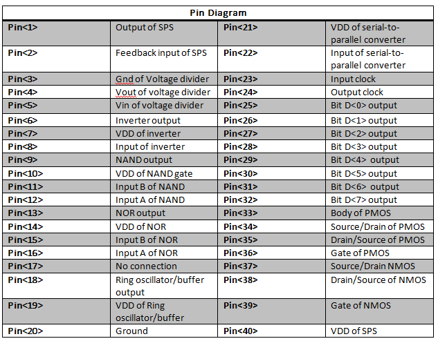
Ground pin<20> 
Connect 5V VDD to pin<19>

Measure the output at pin<10>
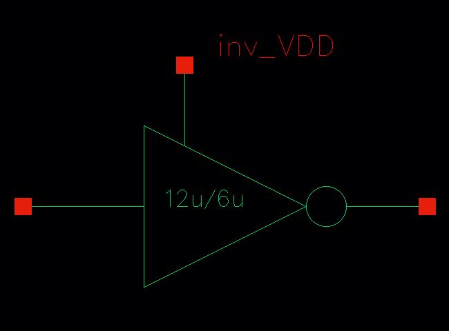


SymbolHow to test
http://cmosedu.com/jbaker/courses/ee421L/f18/students/gebreb1/lab8/NAND.JPG
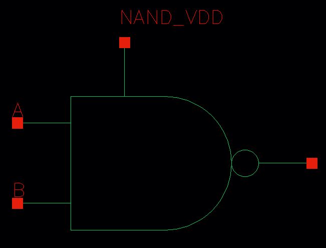
Ground pin<20>
Connect 5V VDD to pin<10>
Apply inputs to pin<11> and pin<12>
Measure the output at pin<9>


SymbolHow to test
http://cmosedu.com/jbaker/courses/ee421L/f18/students/gebreb1/lab8/NOR.JPG
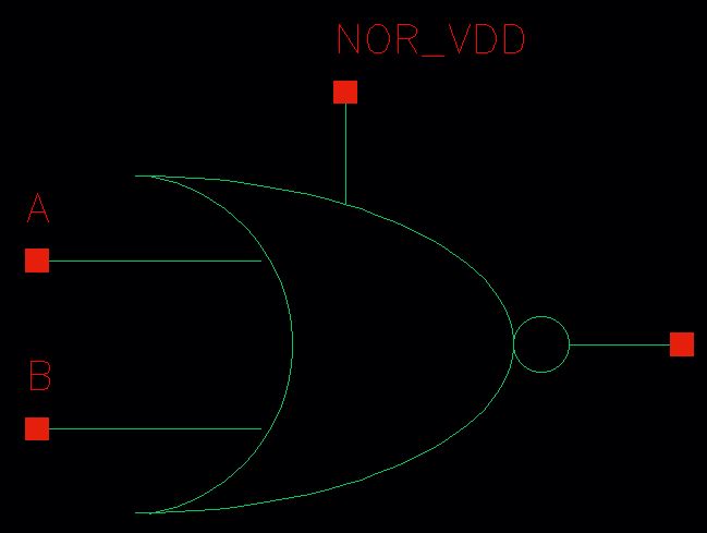
Ground pin<20>
Connect 5V VDD to pin<14>
Apply inputs to pin<15> and pin<16>
Measure the output at pin<13>


SymbolHow to test
http://cmosedu.com/jbaker/courses/ee421L/f18/students/gebreb1/lab8/inverter.JPGGround pin<20>
Connect 5V VDD to pin<7>
Apply input to pin<8> 
Measure the output at pin<6> 


SymbolHow to test
http://cmosedu.com/jbaker/courses/ee421L/f18/students/gebreb1/lab8/PMOS.JPG
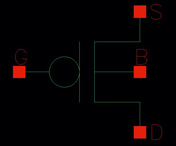
Apply 5V VDD to body at pin<33>
Drain connection at pin<35>
Source connection at pin<34>
Gate input at pin<36>


SymbolHow to test
http://cmosedu.com/jbaker/courses/ee421L/f18/students/gebreb1/lab8/NMOS.JPG
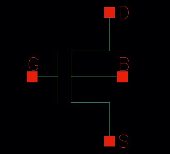
Ground the body at pin<20>
Drain connection at pin<38>
Source connection at pin<37>
Gate input at pin<390-->
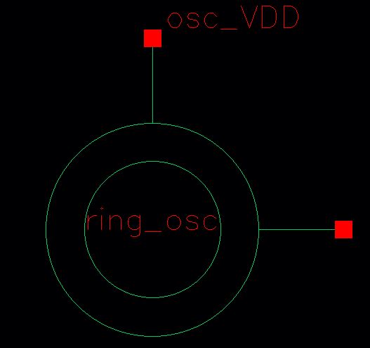


SymbolHow to test
http://cmosedu.com/jbaker/courses/ee421L/f18/students/gebreb1/lab8/V_div.JPG
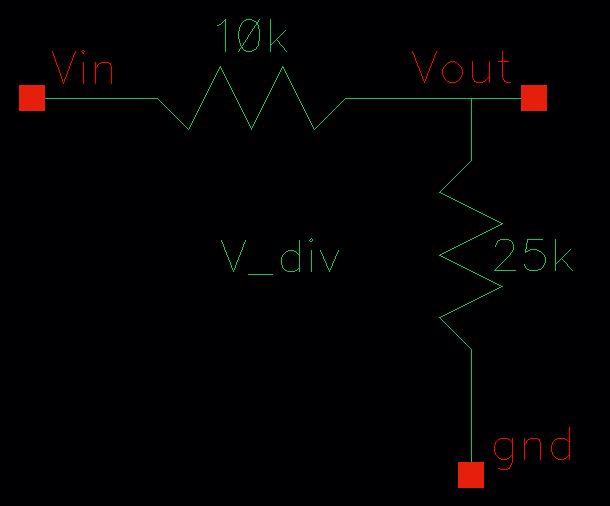
Ground pin<3>
Apply Vin at pin<5>
Measure Vout at pin<4>


SymbolHow to test
http://cmosedu.com/jbaker/courses/ee421L/f18/students/gebreb1/lab8/serial_to_parallel_sym.JPG
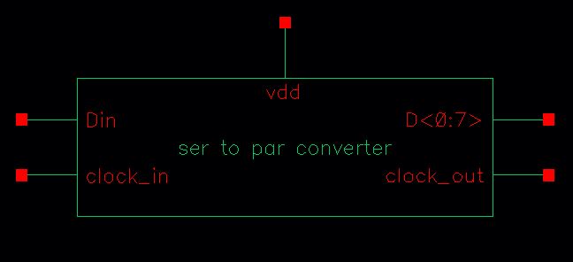
Ground pin<20>
Apply 5V VDD  at pin<21>
Apply input to pin<22>
Apply input clock to pin<23>
Measure the output at pin<25:32>
Measure the clock out at pin<24>


SymbolHow to test
http://cmosedu.com/jbaker/courses/ee421L/f18/students/gebreb1/lab8/SPS_sym.JPG
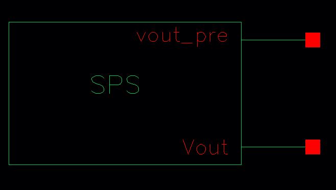
Ground pin<20>
Measure the output od SPS at pin<1>
This Pin connect to a 30uH inductor and to a schottky diode, which is conncected to a 5uF capacitor and 250 Ohm resisstor(load). The node conncected to the capacitor and load resistor is Vout and is used as the feedback into the system of the SPS.
This circuit composes a Boost SPS

Measure the feedback inpu at pin<2>
This pin has label Vout


http://cmosedu.com/jbaker/courses/ee421L/f18/students/gebreb1/lab8/final_drc_lvs.JPG

http://cmosedu.com/jbaker/courses/ee421L/f18/students/gebreb1/lab8/final_lvs.JPG

The pin diagram table is attached  below:
http://cmosedu.com/jbaker/courses/ee421L/f18/students/gebreb1/lab8/pin%20diagram%20table.png


Link to Directory:<<Chip4_f18>>


Return to EE 421 Lab
Return to Student Lab Reports