Lab 8 - EE 421L
Chip files: Chip6_f18.zip
·
Finish Tutorial 6.
Pre-Lab
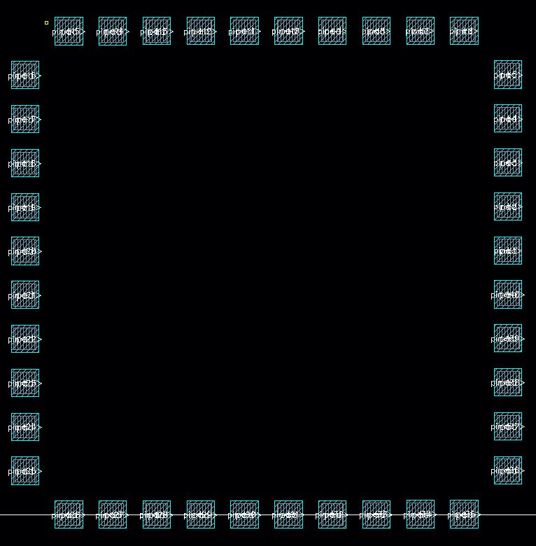
After completing Tutorial 6,
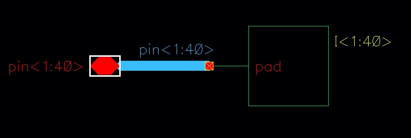
you should wind up with a padframe schematic, symbol,
and layout as seen below:

These will allow us to layout the test chip for the main
content of the lab.
Lab objectives
·
Layout a padframe and test chip layout
including the following:
o One, or more if possible, course
projects.
o A 31-stage ring oscillator
with a buffer for driving a 20 pF off-chip load.
o NAND and NOR gates using 6/0.6
NMOSs and PMOSs.
o An inverter made with a 6/0.6
NMOS and a 12/0.6 PMOS.
o Transistors, both PMOS and
NMOS, measuring 6u/0.6u where all 4 terminals of each device are connected to
bond pads (7 pads + common gnd pad).
§ Note that only one pad is
needed for the common gnd pad. This pad is used to
ground the p-substrate and provide ground to each test circuit.
o Using the 25k resistor laid out
below and a 10k resistor implement a voltage divider (need only 1 more pad
above the ones used for the 25k resistor).
o A 25k resistor implemented
using the n-well (connect between 2 pads but we also need
a common gnd pad).
o Whatever else you would like to
fabricate to use the remaining pins on the chip.
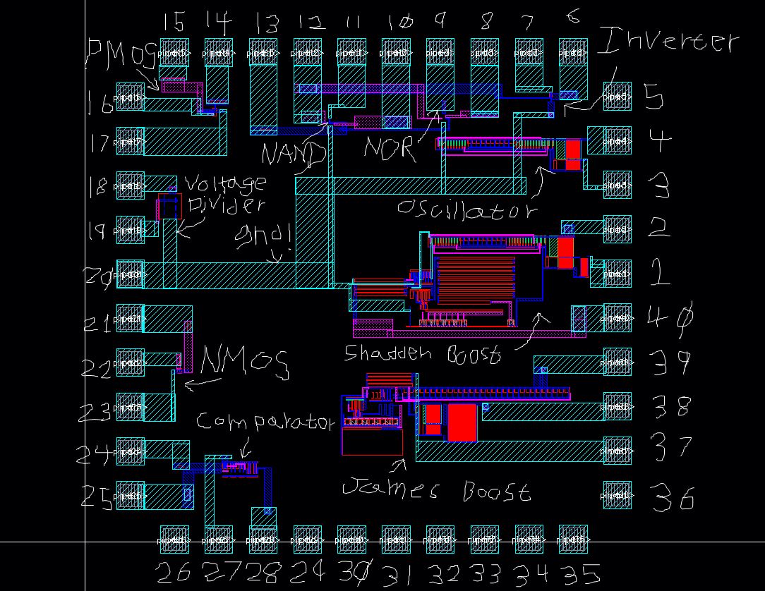
Lab
The design directory for the
test chip can be found here: Chip6_f18.zip.
The main
schematic for the test chip can be seen in the image below:
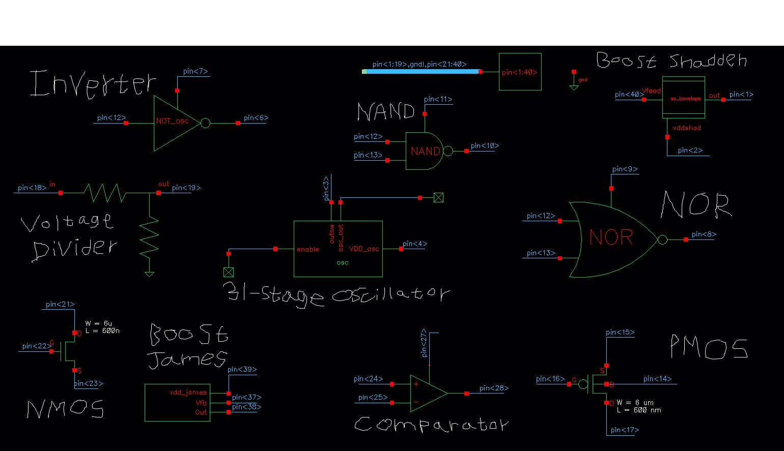
As
seen, our chip includes: James's Boost SPS, Shadden's
Boost SPS, Dylan's Comparator, a 4-terminal PMOS & NMOS, NOR & NAND
gates, an inverter, a 31-stage ring oscillator, and a voltage divider. Note
that Dylan's Boost SPS had to be ommited
since the original layout was slightly
too long to fit on the chip. The previously listed components will be detailed
in the following report. Note that all circuits use the common ground (pin 20)
shown in the above schematic.
James's Boost SPS
James's Boost SPS occupies pins 37, 38, & 39 on the padframe. The schematic can be seen below:
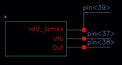
As seen in this image, pin 39 is used for the vdd of the circuit, pin 37 is used for the feedback from
the off-chip circuit (as well as the output of the circuit), and pin 38 is used
for the drain of the switching NMOS of the Boost SPS.
Testing of this chip simply involves supplying the Vs
(between 3.75 - 4.75 V) to pin 39, the negative terminal of the inductor &
Schottky diode to pin 38, the output of the off-chip components to pin
37, and the ground to the common ground (pin 20).
Simulations for testing this circuit can be found in the
included directory under the js_sim_Boost cell.
Shadden's Boost SPS
Shadden's Boost SPS occupies pins
1, 2, & 40 on the padframe. The schematic
can be seen below:
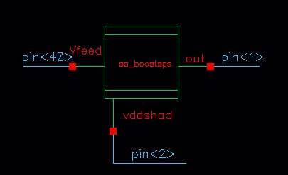
As seen in this image, pin 2 is used for the vdd of the circuit, pin 40 is used for the feedback from
the off-chip circuit (as well as the output of the circuit), and pin 1 is used
for the drain of the switching NMOS of the Boost SPS.
Testing of this chip simply involves supplying the Vs
(between 3.75 - 4.75 V) to pin 2, the negative terminal of the inductor &
Schottky diode to pin 1, the output of the off-chip components to pin 40, and
the ground to the common ground (pin 20).
Simulations for testing this circuit can be found in the
included directory under the sa_sim_Final_symbol_components
cell.
Dylan's Comparator
The comparator occupies pins 24, 25, 27, & 28
on the padframe. The schematic can be seen
below:
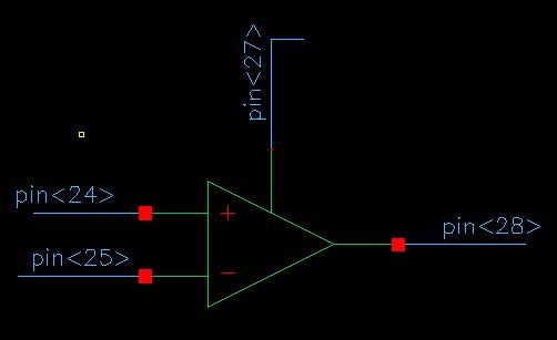
As seen in this image, pin 27 is used for the vdd of the circuit, pin 24 is used for the "plus"
input of the comparator, pin 25 is used for the "minus" input of the
comparator, and pin 28 is used for the output of the comparator.
Testing of this chip simply involves supplying the Vdd to pin 27, the reference input of the comparator to pin
25, the varying input of the comparator to pin 24, the output of the comparator
to pin 28, and the ground to the common ground (pin 20).
Simulations for testing this circuit can be found in the
included directory under the dw_sim_comparator cell.
4-terminal NMOS
The 4-terminal NMOS occupies pins 21, 22, & 23 (note:
the body pin is attached to common ground (pin 20)) on the padframe.
The schematic can be seen below:
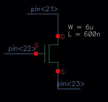
As seen in this image, pin 22 is used for the gate of the
NMOS, pin 21 is used for the drain of the NMOS, and pin 23 is used for the
source of the NMOS.
Testing of this chip simply involves supplying the gate
voltage to pin 22, the drain voltage to pin 21, the source voltage to pin 23,
and the ground to the common ground (pin 20).
4-terminal PMOS
The 4-terminal PMOS occupies pins 14, 15, 16, & 17 on
the padframe. The schematic can be seen below:
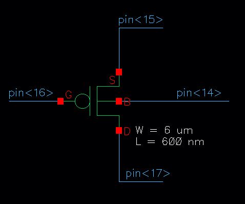
As seen in this image, pin 16 is used for the gate of the
PMOS, pin 17 is used for the drain of the PMOS, pin 15 is used for the
source of the PMOS, and pin 14 is used for the body of the PMOS.
Testing of this chip simply involves supplying the gate
voltage to pin 16, the drain voltage to pin 17, the source voltage to pin 15,
and the vdd (body voltage) to pin 14.
NAND Gate
The NAND gate occupies pins 10, 11, 12, & 13
on the padframe. The schematic can be seen
below:
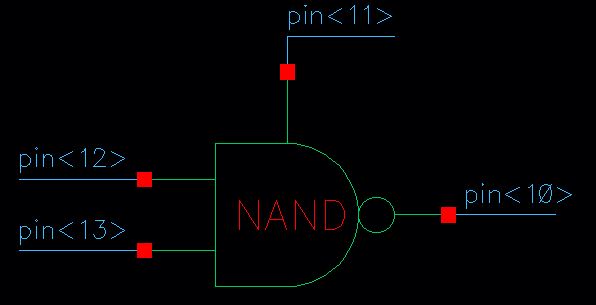
As seen in this image, pin 11 is used for the vdd of the circuit, pins 12 & 13 are used for the
inputs of the NAND gate, and pin 10 is used for the output of the NAND gate.
Testing of this chip simply involves supplying the Vdd to pin 11, the two inputs to pins 12 & 13, the
output of the NAND gate to pin 10, and the ground to the common ground (pin
20).
NOR Gate
The NOR gate occupies pins 8, 9, 12, & 13 on
the padframe. The schematic can be seen below:
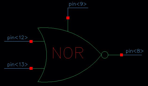
As seen in this image, pin 9 is used for the vdd of the circuit, pins 12 & 13 are used for the
inputs of the NOR gate, and pin 8 is used for the output of the NOR gate.
Testing of this chip simply involves supplying the Vdd to pin 9, the two inputs to pins 12 & 13, the
output of the NOR gate to pin 8, and the ground to the common ground (pin 20).
31-stage Ring Oscillator
The 31-stage ring oscillator occupies pins 3 & 4 on the padframe. The schematic can be seen below:
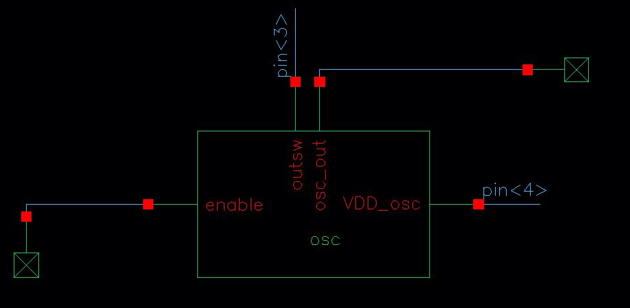
As seen in this image, pin 4 is used for the vdd of the circuit, and pin 3 is used for the output of the
oscillator. The enable and osc_out pins are not used
due to not needing them for the isolated operation of this test circuit.
Testing of this chip simply involves supplying the Vdd to pin 4, the output of the oscillator to pin 3, and
the ground to the common ground (pin 20).
Simulations for testing this circuit can be found in the
included directory under the sa_ring_osc_and_nandsim
cell.
Voltage Divider
The voltage divider occupies pins 18, & 19 on
the padframe. The schematic can be seen below:
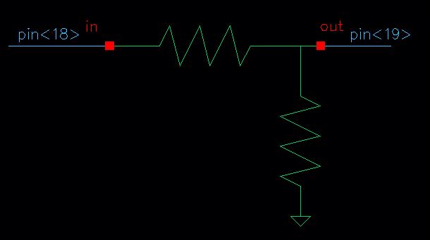
As seen in this image, pin 18 is used for the input of the
voltage divider, and pin 19 is used for the output of the voltage divider.
Testing of this chip simply involves supplying the input of
the voltage divider to pin 18, the output of the voltage divider to pin 19, and
the ground to the common ground (pin 20).
Inverter
The inverter occupies pins 6, 7, & 12 on the padframe. The schematic can be seen below:
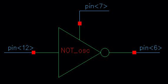
As seen in this image, pin 7 is used for the vdd of the circuit, pin 12 is used for the input of the
inverter, and pin 6 is used for the output of the inverter.
Testing of this chip simply involves supplying the Vdd to pin 7, the input of the inverter to pin 12, the
output of the inverter to pin 6, and the ground to the common ground (pin 20).
Test Chip Layout
The final layout of the test chip onto the padframe can be seen in the image below:
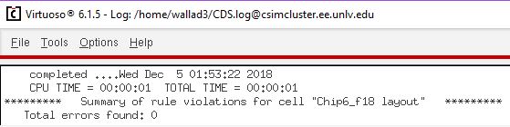
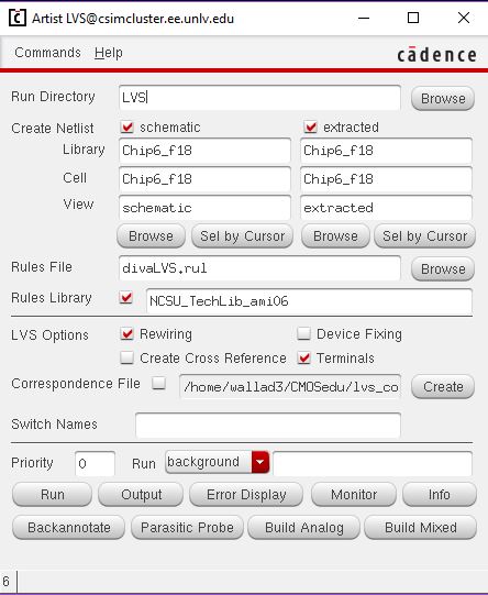
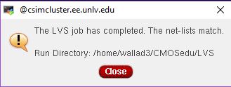
The DRC and
LVS results for the test chip layout can be seen below:
Finally, a pin diagram showing the DIP
package for the manufactured chip is shown below:
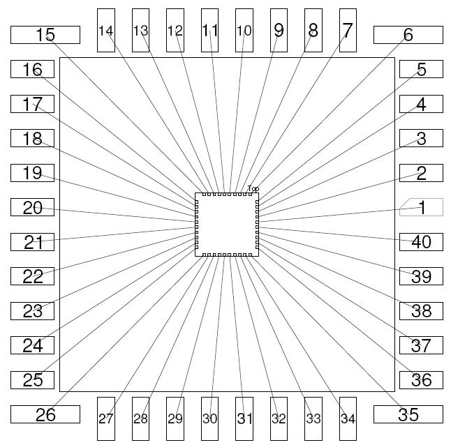
The summary of all pins and their usages
can be seen below (note that some pins are unused due to size constraints of
the chip):
Pin 1: drain of
the switching NMOS for Shadden's Boost SPS
Pin 2: vdd for Shadden's Boost SPS
Pin 3: output
of the 31-stage ring oscillator
Pin 4: vdd of the 31-stage ring oscillator
Pin 5: NOT USED
Pin 6: output
of the inverter
Pin 7: vdd of the inverter
Pin 8: output
of the NOR gate
Pin 9: vdd of the NOR gate
Pin 10: output
of the NAND gate
Pin 11: vdd of the NAND gate
Pin 12: input
of the NAND gate, NOR gate, and inverter
Pin 13: input
of the NAND gate & NOR gate
Pin 14: vdd (body) of the 4-terminal PMOS
Pin 15: source
of the PMOS
Pin 16: gate of
the PMOS
Pin 17: drain
of the PMOS
Pin 18: input
of the voltage divider
Pin 19: output
of the voltage divider
Pin 20: COMMON
GROUND
Pin 21: drain
of the NMOS
Pin 22: gate of
the NMOS
Pin 23: drain
of the NMOS
Pin 24: varying
input of the comparator
Pin 25: fixed
input (reference) of the comparator
Pin 26: NOT
USED
Pin 27: vdd of the comparator
Pin 28: output
of the comparator
Pin 29: NOT
USED
Pin 30: NOT
USED
Pin 31: NOT
USED
Pin 32: NOT
USED
Pin 33: NOT
USED
Pin 34: NOT
USED
Pin 35:
NOT USED
Pin 36: NOT
USED
Pin 37: feedback
& output for James's Boost SPS
Pin 38: drain
of the switching NMOS for James's Boost SPS
Pin 39: vdd for James's Boost SPS
Pin 40:
feedback & output for Shadden's Boost SPS
Again, the complete design directory for the test chip can be downloaded here: Chip6_f18.zip.
This concludes the main content for Lab 8.
Return to
Shadden's Labs
Return to
James's Labs
Return to
Dylan's Labs