EE 421L Digital Integrated
Circuit Design - Lab 7
Using buses and arrays in the design of word
inverters, muxes, and high-speed adders
Authored by
Shadden Abdalla
11/5/18
PRELAB: go
through Tutorial 5.

~~~~~~~~~~~~~~~~~~~~~~~~~~~~~~~~~~~~~~~~~~~~~~~~~~~~~~~~~~~~~~
REAL LAB
Create
schematics and symbols for an 8-bit input/output array of: NAND, NOR, AND,
inverter, and OR gates.
Provide a few simulation examples using these
gates.
Next examine the following schematic.
This is the schematic of a 2-to-1 DEMUX/MUX (and the symbol).
Simulate the operation of this circuit using Spectre
and explain how it works.
Make sure to show, using simulations, how the circuit can be used
for both multiplexing and de-multiplexing.
Create an
8-bit wide word 2-to-1 DEMUX/MUX schematic and symbol.
Include an inverter in your design so the cell
only needs one select input, S (the complement, Si, is generated using an
inverter).
Use simulations to verify the operation of
your design.
Finally, draft the schematic of the full-adder
seen in Fig. 12.20 using 6u/0.6u devices (both PMOS and NMOS).
Create an adder symbol for this circuit (see
the symbol used in lab6).
Use this symbol to draft an 8-bit adder
schematic and symbol.
For how to label the bus so the carry out of
one full-adder goes to the carry in of another full-adder review the ring
oscillator schematic discussed in Cadence Tutorial 5.
Simulate the operation of your 8-bit
adder.
Lay out this 8-bit adder cell (*note* that
this is the only layout required in this lab).
Show that your layout DRCs and LVSs
correctly.
~~~~~~~~~~~~~~~~~~~~~~~~~~~~~~~~~~~~~~~~~~~~~~~~~~~~~~~~~~~~~~~~~~~~~~~~~~~~~~~~~~~~~~~~~~~~~~~~~~~~~~~~
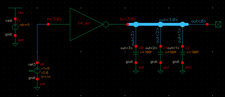
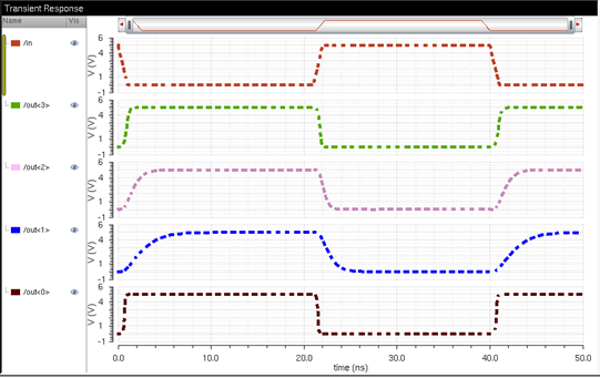
4 BIT INVERTER
I created an
inverter with a four bit input and a four bit output
and made a symbol with my initials in it.
Simulating the
schematic using three capacitors for 3 of the outputs and a noconn
from the basic library for one of the outputs. The input of the inverter is a
pulsing voltage source. I connected the VDD to a vdc of 5 volts instead of
creating a stimuli. The output is split up into
families below and is as expected in Dr. Baker’s simulation.
~~~~~~~~~~~~~~~~~~~~~~~~~~~~~~~~~~~~~~~~~~~~~~~~~~~~~~~~~~~~~~~~~~~~~~~~~~~~~~~~~~~~~~~~~~~~~~~~~~~~~~~~
Part 1: 8-BIT GATES
~~~~~~~~~~~~~~~~~~~~~~~~~~~~~~~~~~~~~~~~~~~~~~~~~~~~~~~~~~~~~~~~~~~~~~~~~~~~~~~~~~~~~~~~~~~~~~~~~~~~~~~~
CREATE SCHEMATICS AND SYMBOLS FOR AN 8 BIT-NAND
1-BIT NAND
First I created a regular nand and then
connected the <7:0> NAND to <7:0> busses.


8-BIT NAND
Below, I
instantiated the NAND as an 8 bit component and then
added 8 bit busses to it so that each node carries 8 bits of wire. Then I added
my initials to my nand using a label.
is the 8 bit nand after I created the 1 bit nand,
with the symbol next to it.


~~~~~~~~~~~~~~~~~~~~~~~~~~~~~~~~~~~~~~~~~~~~~~~~~~~~~~~~~~~~~~~~~~~~~~~~~~~~~~~~~~~~~~~~~~~~~~~~~~~~~~~~
CREATE SCHEMATICS AND SYMBOLS FOR AN 8-BIT NOR
1-BIT NOR
Below is the
simple, one bit NOR that I created.


8-BIT NOR
Below is the 8-bit
NOR that I created using the same method that I used with the NAND, and
instantiated the component as a 8-bit component.


~~~~~~~~~~~~~~~~~~~~~~~~~~~~~~~~~~~~~~~~~~~~~~~~~~~~~~~~~~~~~~~~~~~~~~~~~~~~~~~~~~~~~~~~~~~~~~~~~~~~~~~~
CREATE SCHEMATICS AND SYMBOLS FOR 8 BIT AND
1-BIT AND
I created an
AND by inverting the NAND I made in the previous lab.


8-BIT AND
I made it an 8
bit AND by instantiating it as an 8 bit component and then
adding 8 bit pins and an 8 bit bus.


~~~~~~~~~~~~~~~~~~~~~~~~~~~~~~~~~~~~~~~~~~~~~~~~~~~~~~~~~~~~~~~~~~~~~~~~~~~~~~~~~~~~~~~~~~~~~~~~~~~~~~~~
CREATE SCHEMATICS AND SYMBOLS FOR AN 8-BIT NOR
1-BIT NOR
I created an
OR symbol by inverting the NOR I made in the previous lab as well.


8-BIT NOR
Then I
instantiated the OR as an 8-bit component using 8 bit
input output pins and 8 bit bus.


~~~~~~~~~~~~~~~~~~~~~~~~~~~~~~~~~~~~~~~~~~~~~~~~~~~~~~~~~~~~~~~~~~~~~~~~~~~~~~~~~~~~~~~~~~~~~~~~~~~~~~~~
CREATING SCHEMATICS AND SYMBOLS FOR AN 8-BIT
INVERTER
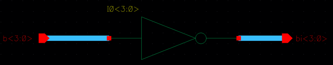
1-BIT INVERTER
Then I created
an inverter and a symbol for it. I don’t have my layout for the inverter here
because I created it from scratch for my layout. You can see both inverters in
my full adder layout.


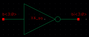
8-BIT INVERTER
I made it an
8-bit inverter the same way I did in previous components and the symbols.


~~~~~~~~~~~~~~~~~~~~~~~~~~~~~~~~~~~~~~~~~~~~~~~~~~~~~~~~~~~~~~~~~~~~~~~~~~~~~~~~~~~~~~~~~~~~~~~~~~~~~~~~
PART 2:
SIMULATING THE 8-BIT GATES
~~~~~~~~~~~~~~~~~~~~~~~~~~~~~~~~~~~~~~~~~~~~~~~~~~~~~~~~~~~~~~~~~~~~~~~~~~~~~~~~~~~~~~~~~~~~~~~~~~~~~~~~
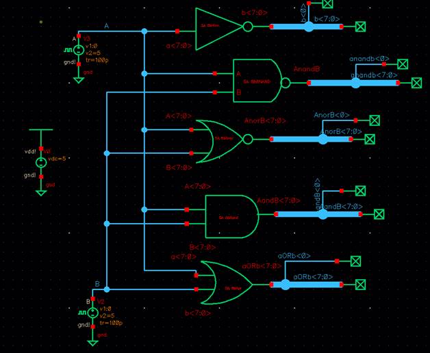
I simulated
all the gates that I made above using two pulsing inputs A and B and a VDD.
From top to bottom I have an 8-bit inverter, 8-bit NAND, 8-bit NOR, 8-bit AND and 8-bit OR.

~~~~~~~~~~~~~~~~~~~~~~~~~~~~~~~~~~~~~~~~~~~~~~~~~~~~~~~~~~~~~~~~~~~~~~~~~~~~~~~~~~~~~~~~~~~~~~~~~~~~~~~~
PART 3: 2-1 MUX
/ DEMUX
~~~~~~~~~~~~~~~~~~~~~~~~~~~~~~~~~~~~~~~~~~~~~~~~~~~~~~~~~~~~~~~~~~~~~~~~~~~~~~~~~~~~~~~~~~~~~~~~~~~~~~~~
Below is the
schematic for the mux/ demux. It is created using two
transmission gates that are not on at the same time; when one is on the other
one is off. When S is at 0, the bottom gate is on and the top gate is off, and
when S is 1 the bottom gate is off and the top gate is
on. When the top gate is on, A is connected to the output. When the bottom gate
is on B is connected to the output. Si is the inverse of S. Demultiplexing
means that the control uses Z as the input and sends it to either A or B. The
demultiplexing circuit is when you connect the S to the input of the inverter.
The output of the inverter feeds into Si. Instead of having the S at the bottom
I have it feeding into the inverter input.


The demux was created by inverting the mux that I created
earlier.


Simulating the
mux to see if it was working. You can see based on the response that it is
working properly.


Creating an
8-bit wide mux/demux
I created an
8-bit wide mux/demux by instantiating the mux/demux as an 8-bit component, with 8-bit input output pins
and an 8-bit bus.


Simulating the 8-bit wide mux/demux
I then
simulated the 8bit wide mux/demux that I just
created. I used two pulsing input sources A and B with an 8
bit output for one of them. The other one has 8 bit
inputs and one bit outputs.


~~~~~~~~~~~~~~~~~~~~~~~~~~~~~~~~~~~~~~~~~~~~~~~~~~~~~~~~~~~~~~~~~~~~~~~~~~~~~~~~~~~~~~~~~~~~~~~~~~~~~~~~
PART 4: AOI FULL ADDER
~~~~~~~~~~~~~~~~~~~~~~~~~~~~~~~~~~~~~~~~~~~~~~~~~~~~~~~~~~~~~~~~~~~~~~~~~~~~~~~~~~~~~~~~~~~~~~~~~~~~~~~~
I created the schematic for an
AND OR INVERT (AOI) full adder using Dr. Baker’s design from the CMOS book.
This full adder has a lower delay than the one we created in lab 6. I also
created the symbol shown on the right.


Layout – I
created the layout using multipliers for my PMOS and NMOS devices. The two
inverters are shown on the right and left of the layout.

I performed a DRC and there were no errors.
![]()
Extracted – I
extracted the layout to prepare for LVS.

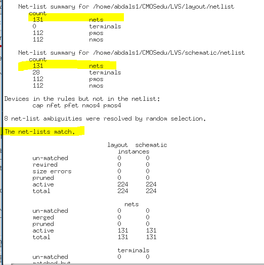
LVS – the
netlists matched.


~~~~~~~~~~~~~~~~~~~~~~~~~~~~~~~~~~~~~~~~~~~~~~~~~~~~~~~~~~~~~~~~~~~~~~~~~~~~~~~~~~~~~~~~~~~~~~~~~~~~~~~~
PART 5: 8-BIT AOI FULL ADDER
~~~~~~~~~~~~~~~~~~~~~~~~~~~~~~~~~~~~~~~~~~~~~~~~~~~~~~~~~~~~~~~~~~~~~~~~~~~~~~~~~~~~~~~~~~~~~~~~~~~~~~~~
I then created
an 8-bit version of the full adder using the symbol that I created above,
instantiating the component, the busses and the pins as 8-bit pieces. Then I
created the symbol.


Simulating the
8 bit adder using the numbers 11100000 (input A) and
00001111 (input B). I added the two together using the full adder and received
the correct answer, 11101111 as seen in the response below. The response is
expressed in all 8 bits of Z so you can follow the
order below to read the output. A high is a logic 1 and a low is a logic 0. A
high is expressed as the number 5 in the transient response.


8 BIT LAYOUT
I connected the outputs of each
full adder to the input of the next one and left the first cin
open and the last cout open. The following two photos
show a zoomed in version of my layout. I used metal 3 and metal 2 for my final
connections.

Whole 8-bit layout. This shows the entire zoomed
out layout.

I performed a
DRC and there were no errors.

Extracted 8-bit layout, ready for LVS.

LVS - the
netlists match.

I backed up my
files into my google drive.

~~~~~~~~~~~~~~~~~~~~~~~~~~~~~~~~~~~~~~~~~~~~~~~~~~~~~~~~~~~~~~~~~~~~~~~~~~~~~~~~~~~~~~~~
Return to Fall
2018 421L Students
~~~~~~~~~~~~~~~~~~~~~~~~~~~~~~~~~~~~~~~~~~~~~~~~~~~~~~~~~~~~~~~~~~~~~~~~~~~~~~~~~~~~~~~~