EE 421L
Digital Integrated Circuit Design - Lab 2
Design of a 10-bit digital-to-analog converter (DAC)
Shadden Abdalla
Abdals1@unlv.nevada.edu
PRELAB WORK
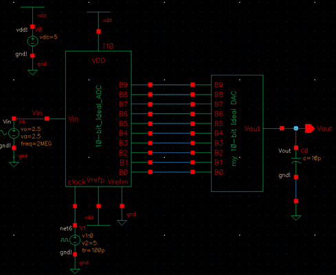
The relation
between Vin B[9:0] and Vout:
The ADC captures a
voltage at specific instances in time, the ADC reads Vin, and then converts Vin
into a binary 10-bit number. Then the DAC reads the 10-bit number outputs the
voltage at multiples of the LSB. Vout is a multiple
of the LSB (4.88mV in this case). The output staircases at increments of
4.88mV, or at increments of the LSB.
Download lab2 file
and extract it.

Define the file in
cds.lib library
![]()
Open up the sim_Ideal_ADC_DAC schematic cell, launch ADE L, load state
and output the Vin and Vout simulations of the
schematic.
 è
è  è
è 
Colors changed to show understanding of graph properties.
Below is the same
circuit’s simulation except for with a different input voltage. I changed the
amplitude and the offset to 5mV each.


------------------------------------------------------------------------------------------
REAL LAB WORK
This lab is the
creation of a 10-bit DAC using n-well resistors following CMOS book topology
from figure 30.14:
 Calcul
 ating least significant bit (LSB) using
this formula.
ating least significant bit (LSB) using
this formula.
VDD= 5V, N=10.
LSB = 5V / 2^(10) = 5V / 1024 =
4.88mV
Schematic of 4.88mV = LSB shown on the
top of the square wave

 Schematic checked with no errors.
The design of a 10-bit DAC using an n-well R of 10k.

I created the schematic
and checked and saved.
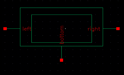
SYMBOL 1:
Below is the symbol compared to the ideal one already
given to me. I used the same size as the one already made.

Above is my finished
symbol of the resistor part of the DAC. I am going to connect ten of them
together to create the 10-bit DAC.
Below is the 10-bit DAC
using the DAC symbol that I made. I connected them all together from B9-B0 and
then connected the bottom of B0 to a 10k resistor and ground.


Regular size above. Above is the zoomed in version broken into
two parts.
SYMBOL 2:
Below is the symbol I made for the 10
bit DAC that I made above, compared to the one that was given to me in
lab two (the ideal one).

 ç my new symbol
I moved the shape from
the ideal one and copied it into my 10 bit DAC (and
the pins from my schematic) and then renamed the symbol and deleted the ideal
DAC symbol remains that I didn’t need.
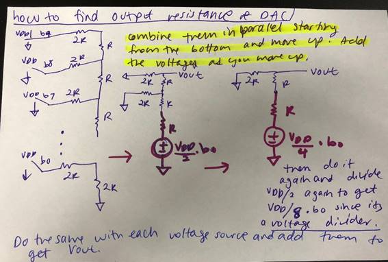
HOW TO DETERMINE THE
OUTPUT RESISTANCE OF THE DAC, R, BY COMBINING RESISTORS IN PARALLEL AND SERIES.
The circuit is a voltage
divider that moves upwards. A voltage divider with two equal values of
resistance has a Vout = (Vin/2)*bx
thus the output after moving up once and combining the resistances using a
voltage divider is VDD/2*bx. The x denotes any value of b that moves upward,
depending how many bits are in the circuit. Since the DAC has ten bits, it will
move upwards from b0 to b9. Every time you move up, you will continue to divide
the voltage by two while making sure to multiply by the value bx of that
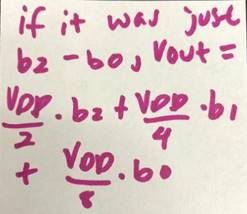
specific isntance. If the circuit started at b0 and
ended at b2, you would use three voltage dividers and divide the VDD 3 times.
The first time the input will equal b2*(VDD/2), the second time will result in
b1*(VDD/4). The third time the answer will also divide again by two and equal
b0*(VDD/8).
DELAY, DRIVING A LOAD.
Ground all DAC inputs except B9. Connect B9 to a pulse source (0 to VDD) and
show, and predict using 0.7RC, the delay the DAC has driving a 10pF load.
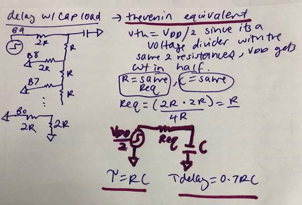
Calculating the time
delay: ![]() è
è ![]() =
69.9 nanoseconds
=
69.9 nanoseconds


A delay of 69.9n is shown above in the
capacitor with the simulation shown to its right
CAPACITIVE LOAD
Adding a 10pF capacitive
load changes the phase of the output in comparison to the input voltage. The
output lags the input by about 69 nanoseconds which mirrors the time delay that
we inputted earlier onto the capacitor. The input reaches peak at about
629.48ns and the output reaches peak at about 699.317ns, showing that they are
out of phase by about 70nanoseconds which is consistent with the above
capacitor delay. It is interesting, because even without adding the delay, the
circuit lagged the input the same amount.

NO LOAD
Now I’m going to copy my
design into the original schematic, renamed sim2 so that I know the difference
and will test to see if my schematic works just as well as the original.

Below is the result with
my DAC Below
is the original circuit from the ideal DAC


The results are
the same and as expected, showing that the DAC I made works under no load.
RESISTOR
Adding a 10 kohm resistive load below. Adding the resistor cuts the
output voltage in half at the peak but the trough of the graph stayed the same.
They are also in phase and created a voltage divider at the output.


RESISTOR AND CAPACITOR
Adding both
components from the above circuit, a resistor and capacitor load, changes the
output much more drastically than adding one or the other. The input reaches
peak at about 629.481us where the output reaches peak at about 676.076us which
shows a delay between the input and output of about 47microseconds.


- In a real circuit the switches seen above
(the outputs of the ADC) are implemented with transistors (MOSFETs).
- Discuss what happens if the resistance of the switches
isn't small compared to R.
If
the resistance is not small compared to R, the overall resistance will increase
which will reduce the size of the output voltage that the circuit will produce
since more of the voltage will dissipate within the resistance. Less resistance
will allow more voltage to output whereas more resistance will cause some of
the voltage to dissipate before it can output.
 I then backed up my work, zipped it up and
put it in my google drive.
I then backed up my work, zipped it up and
put it in my google drive.
Return to Dr.
Baker's Students