Lab 5 - ECE 421L
Authored
by Byron Gorsuch,
gorsuch@unlv.nevada.edu,
10/11/2017
This
lab demonstrates how to draft schematics, layouts and symbols for two
inverters with sizes of 12u/6u and 48u/24u, as well as how to simulate
and verify the schematics.
Prelab
Tutorial 3 was followed in order to layout and design a 12u/6u PMOS/NMOS inverter.


Figure 1: 12u/6u Inverter Schematic Figure 2: 12u/6u Inverter Layout
Figure 3: 12u/6u Extracted
Figure 4: 12u/6u
Inverter Symbol


Figure 5: 12u/6u DRC
Figure 6: 12u/6u LVS
Lab Work
A 48u/24u inverter was drafted in a simlar fashion to the 12u/6u inverter. In order to
expand the NMOS and PMOS for the inverter to the right widths, a
multiplier of 4 was used. This created 4 total MOSFETS per device which
were then connected as shown in the following layout.


Figure 7: 48u/24u Inverter Schematic
Figure 8: 48u/24u
Layout
Figure 9: 48u/24u Extracted
Figure
10: 48u/24u Inverter Symbol


Figure 11:
48u/24u DRC
Figure 12:
48u/24u LVS
Once the two inverters were
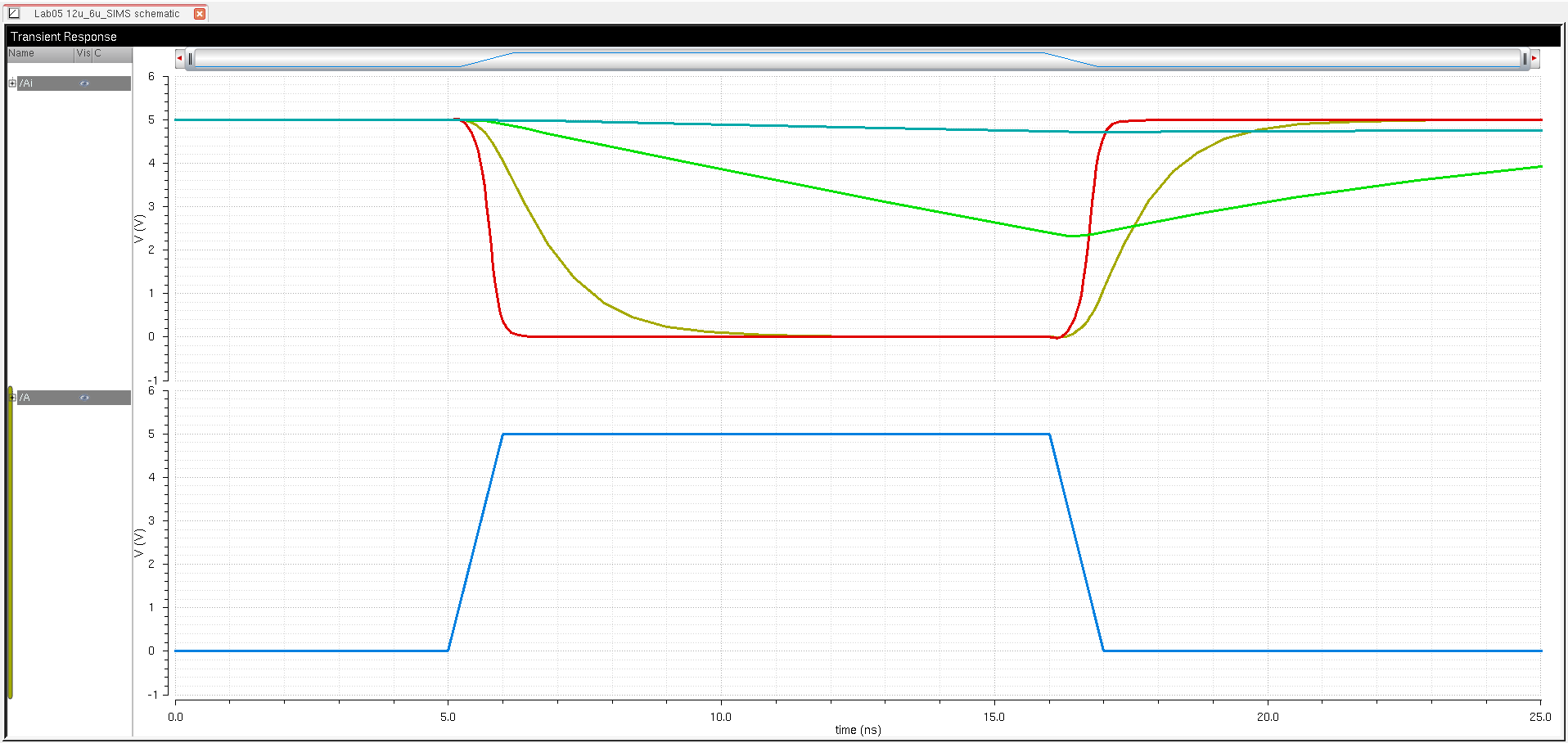
drafted and verified, a parametric analysis was performed on a test
circuit which used the schematics to drive capacitors of values: 100fF,
1pF, 10pF, and 100pF. The simulations were performed using both the
Spectre and Ultrasim simulators however, there seems to be no noticable
difference between the two.


Figure
13: Schematic for Testing 12u/6u Inverter
Figure
14: Spectre Simulation Results for 12u/6u Inverter

Figure 15:
Ultrasim Simulation Results for 12u/6u Inverter


Figure 16: Schematic for Testing 48u/24u Inverter
Figure
17: Spectre Simulation
Results for 48u/24u Inverter

Figure 15: Ultrasim Simulation Results for 48u/24u Inverter
As
can be seen from the simulations, as the capacitive load increases, the
inverter's response slows down. Furthermore, the performance of the
48u/24u inverter is much better than the 12u/6u inverter since the
48u/24u inverter is able to distribute the load accross its four
MOSFETs.
A zip folder of these schematics can be found HERE
Return to my lab directory
Return to CMOSedu.com