Lab 4 - ECE 421L
Authored
by Byron Gorsuch,
gorsuch@unlv.nevada.edu,
September 26, 2017
This
lab demonstrates how to layout, using Virtuoso, NMOS and PMOS devices
using ON's C5 process, as well as how to determine the devices' IV
characteristics using the Spectre simultor.
Prelab
Tutorial 2
was followed in order to create the schematics, symbols and layouts for
the PMOS and NMOS devices that will be used throughout the lab.


Figure 1: NMOS Schematic
Figure 2: NMOS Symbol
Figure 3: NMOS Layout


Figure
4: PMOS Schematic
Figure 5: PMOS
Symbol
Figure 6: PMOS Layout
Lab Work
- Generate 4 schematics and simulations (see the examples in the Ch6_IC61 library, but note that for the PMOS body should be at vdd! instead of gnd!):
- A schematic for simulating ID
v. VDS of an NMOS device for VGS varying from 0 to 5 V in 1 V steps
while VDS varies from 0 to 5 V in 1 mV steps. Use a 6u/600n
width-to-length ratio


Figure
7: Schematic Used to Simulate ID vs VDS
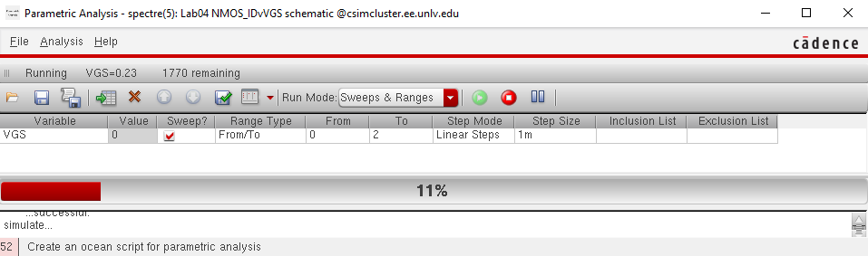
Figure 8: Setting up Parametric
Simulation
 Figure 9: ID vs VDS Simulation Results
- A
schematic for simulating ID v. VGS of an NMOS device for VDS = 100 mV
where VGS varies from 0 to 2 V in 1 mV steps. Again use a 6u/600n
width-to-length ratio.

Figure
10: Schematic for Simulating ID vs VGS
Figure 11: Parametric Analysis for ID vs VGS
 Figure 12: ID vs VGS Simulation Results
- A
schematic for simulating ID v. VSD (note VSD not VDS) of a PMOS device
for VSG (not VGS) varying from 0 to 5 V in 1 V steps while VSD varies
from 0 to 5 V in 1 mV steps. Use a 12u/600n width-to-length ratio.

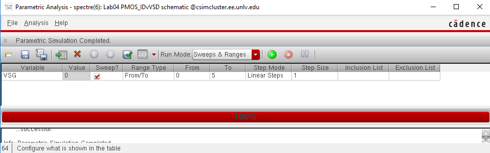
Figure 13: Schematic for ID
vs VSD
Figure 14: Parametric Analysis for ID vs VSD
 Figure 15: ID vs VSD Simulation Results
- A
schematic for simulating ID v. VSG of a PMOS device for VSD = 100 mV
where VSG varies from 0 to 2 V in 1 mV steps. Again, use a 12u/600n
width-to-length ratio.

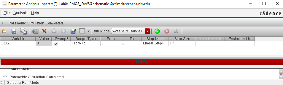
Figure 16: Schematic for ID
vs VSG
Figure 17: Parametric Analysis for ID vs VSG
 Figure 18: ID vs VSG Simulation Results
- Lay
out a 6u/0.6u NMOS device and connect all 4 MOSFET terminals to probe
pads (which can be considerably smaller than bond pads [see MOSIS design rules] and directly adjacent to the MOSFET (so the layout is relative small).


Figure
19: NMOS Probe Pad Layout Close-up
Figure 20: Full Layout of NMOS with Probe
Pads
- Show your layout passes DRCs.


Figure
21: Successful DRC
Figure 22: Extracted View of NMOS with Pads
- Make a corresponding schematic so you can LVS your layout.


Figure
23: Schematic of NMOS with Probes
Figure 24: Successful LVS for NMOS with Probe Pads
- Lay out a 12u/0.6u PMOS device and connect all 4 MOSFET terminals to probe pads.


Figure 25: PMOS Probe Pad
Layout Close-up
Figure 26: Full Layout of PMOS
with Probe Pads
- Show your layout passes DRCs.


Figure
27: Successful DRC
Figure 28: Extracted View of PMOS with Pads
- Make a corresponding schematic so you can LVS your layout.


Figure
29: Schematic of PMOS with Probes
Figure 30: Successful LVS for PMOS with Probe Pads
Return to my lab directory
Return to CMOSedu.com


