Lab 07 - EE 421L
Authored :: Aaron Escobedo
Email :: Escoba3@UNLV.Nevada.edu
Due :: November 8th, 2017
Lab
description
This lab will familiarize ourselves with the design using busses, arrays, word inverters, muxes, and high-speed adders..
Prelab
We will begin our lab by completing the tutorial 5 set up on the cmosedu.com website; below is now some of my completed work.
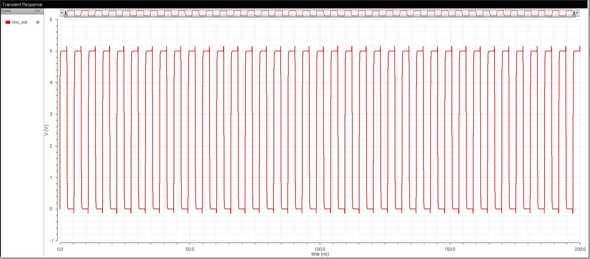
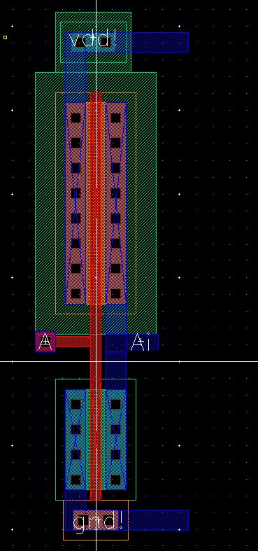
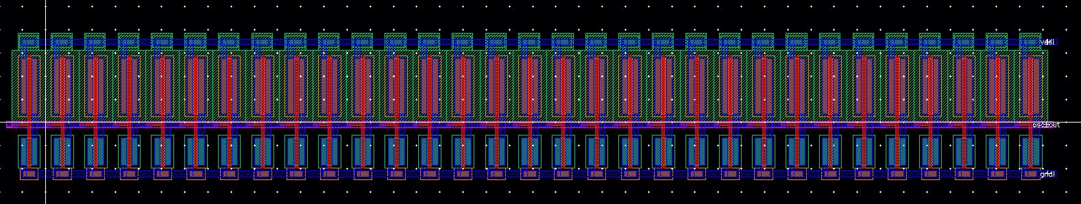
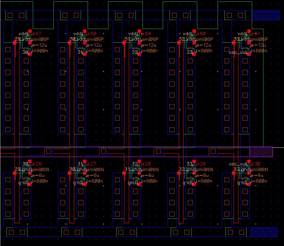
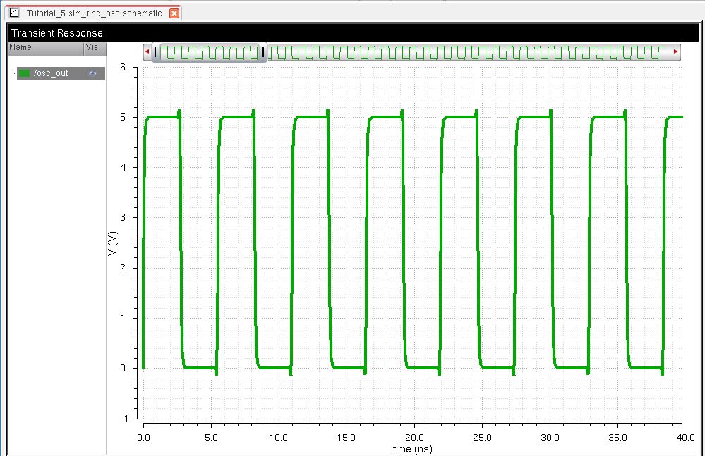
Initially, we want to place 31 inverters in series to create a ring oscillator
We can clearly see, they produce the same results, however, one is much easier to place in a large circuit.
From here, we should try to create a layout for these circuits - which can lead us to learn a few new tricks.
Lab Work
Now
that we have become familar with how to create some busses, we can
begin using them to implement some of the logic gates we previously
developed
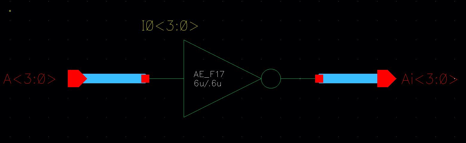
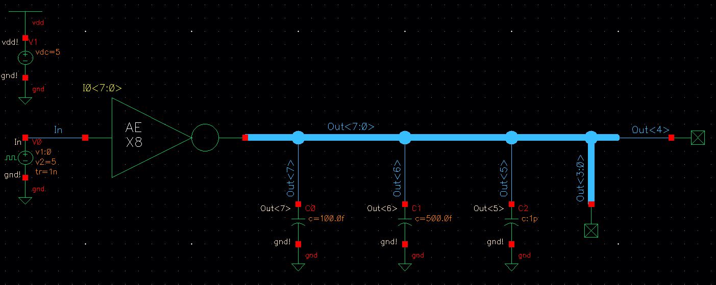
To start, we will need to create another inverter, but this time, with a 6/.6 width for the NMOS and PMOS appropiately;

6/0.6 Inverter Schematic | 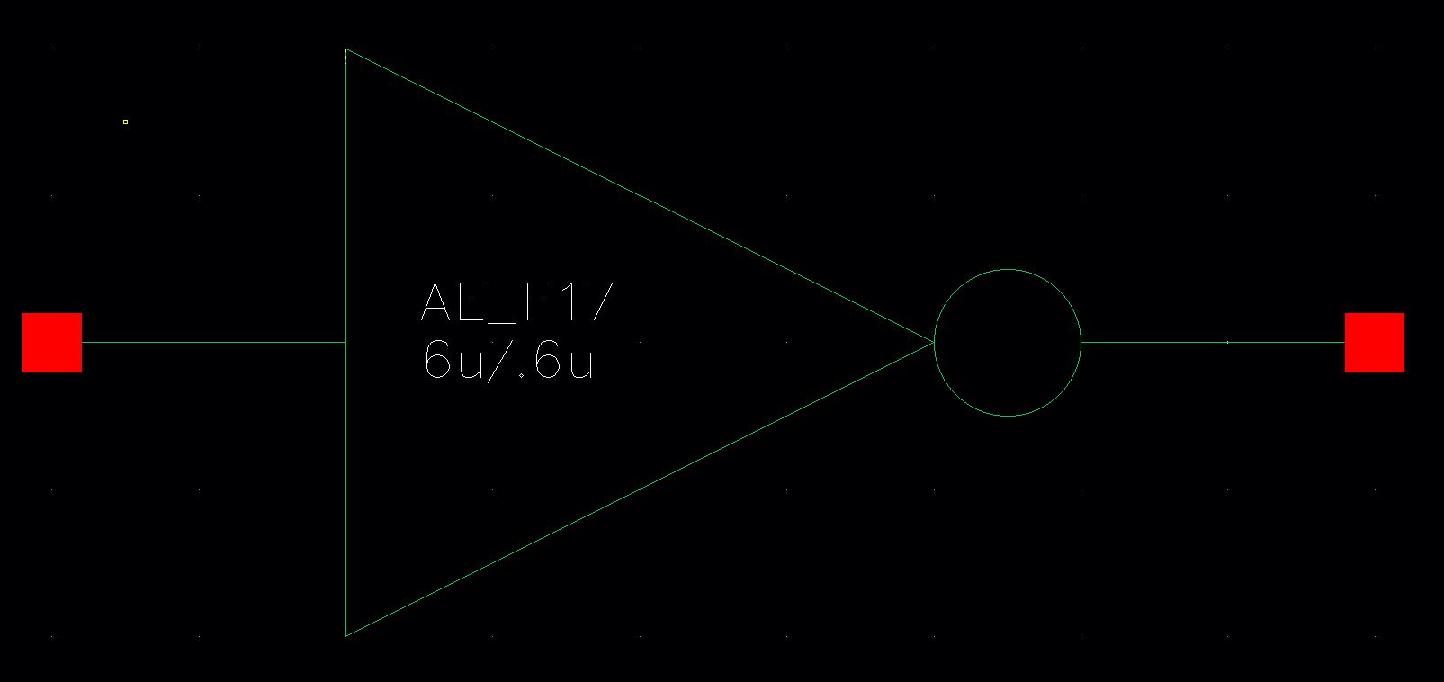
Associated Symbol
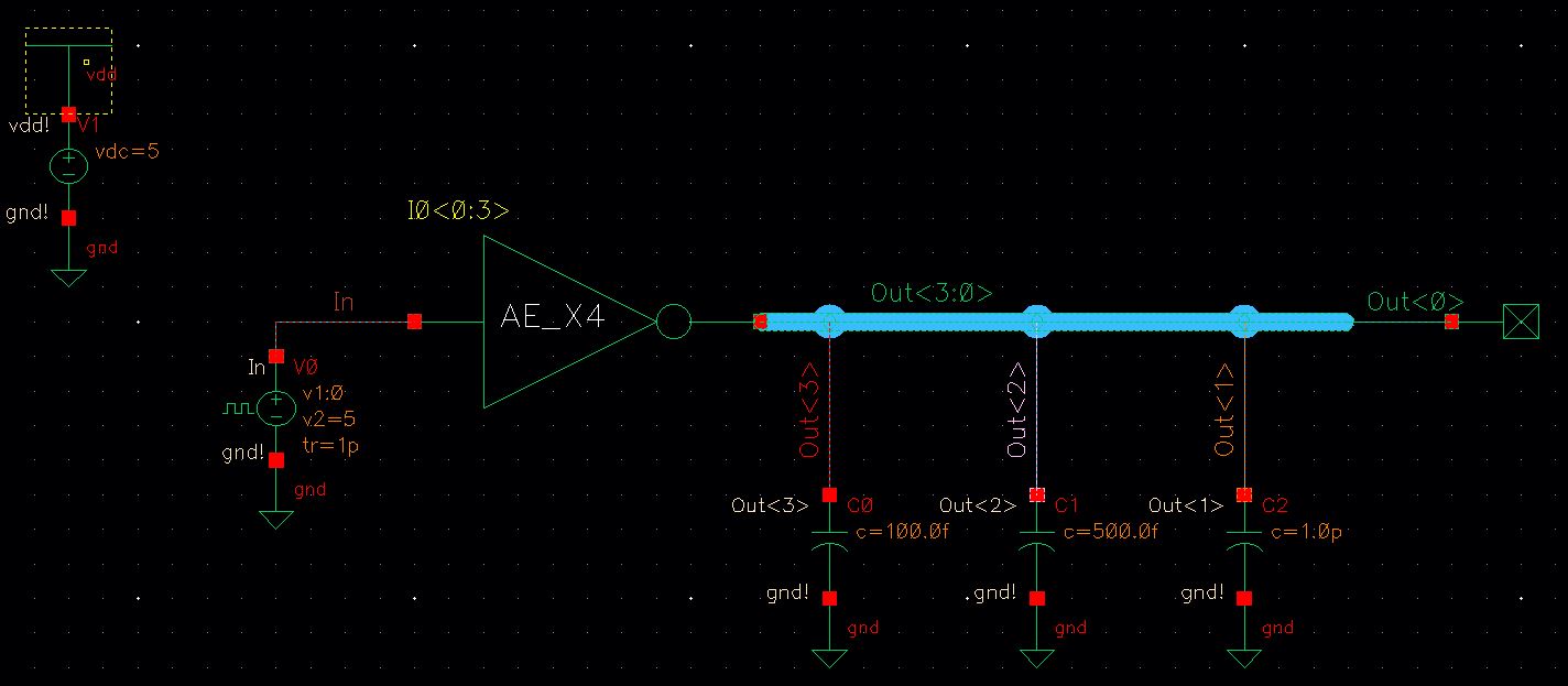
|

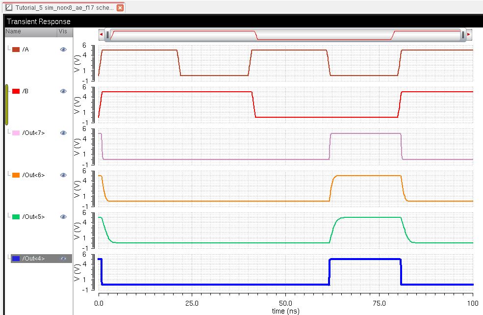
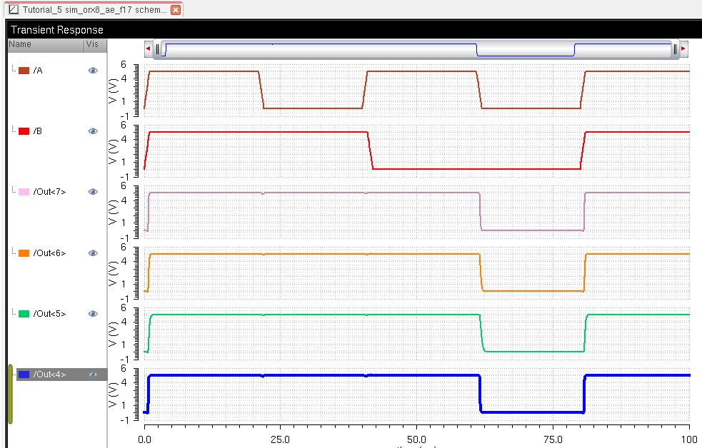
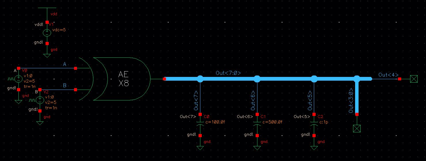
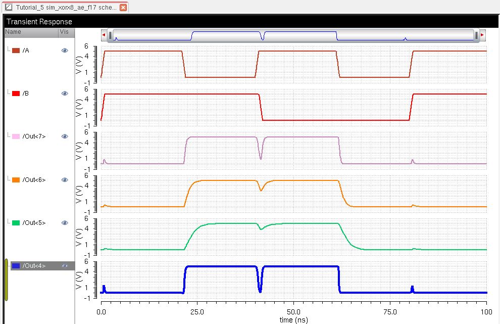
General outputs - we can see the delay difference between each node due to capacitors | 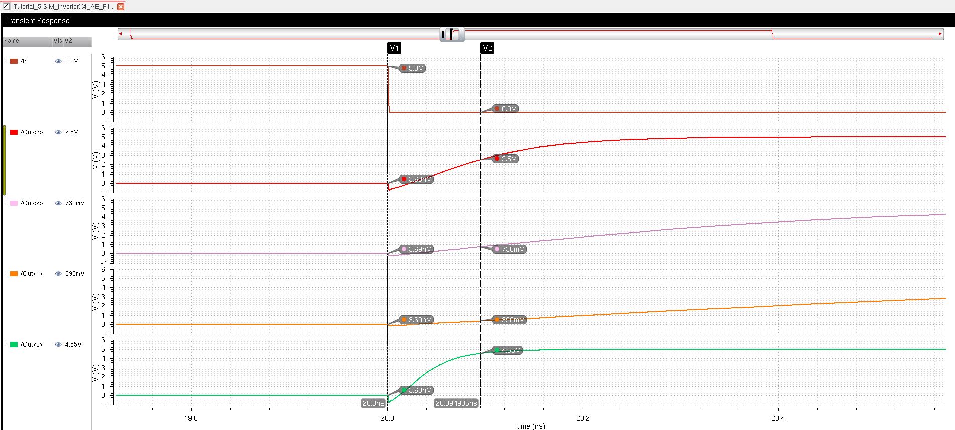
Zoomed in - we can see at Out<3>, it reached 1 time constants, while Out<2> and Out<1> are much slower |
Clearly,
since the capacitor on Out<3> is the smallest and become larger
across each node, we can conclude that a smaller capacitor will result
ina faster transition to a final voltage. This follows from our lessons
taught about rise times across capacitors.
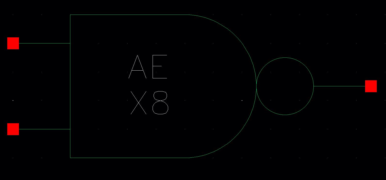
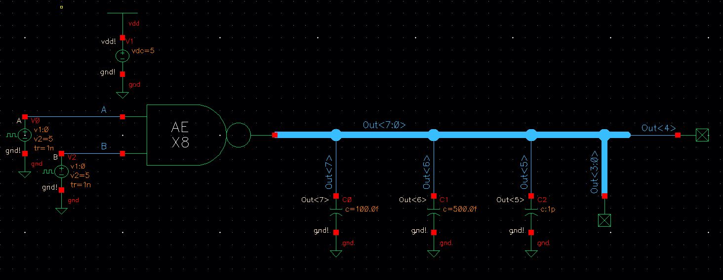
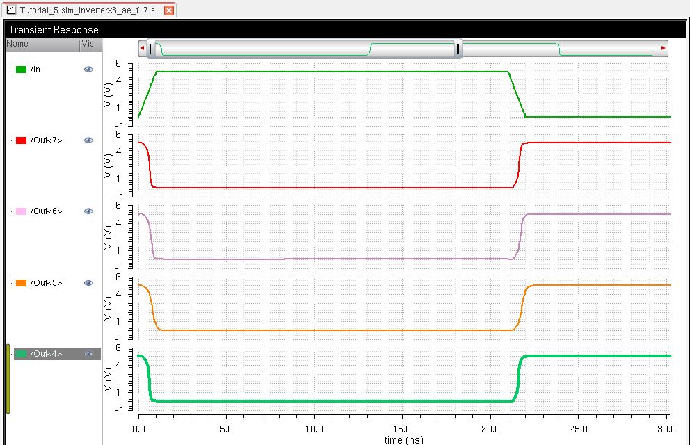
Now
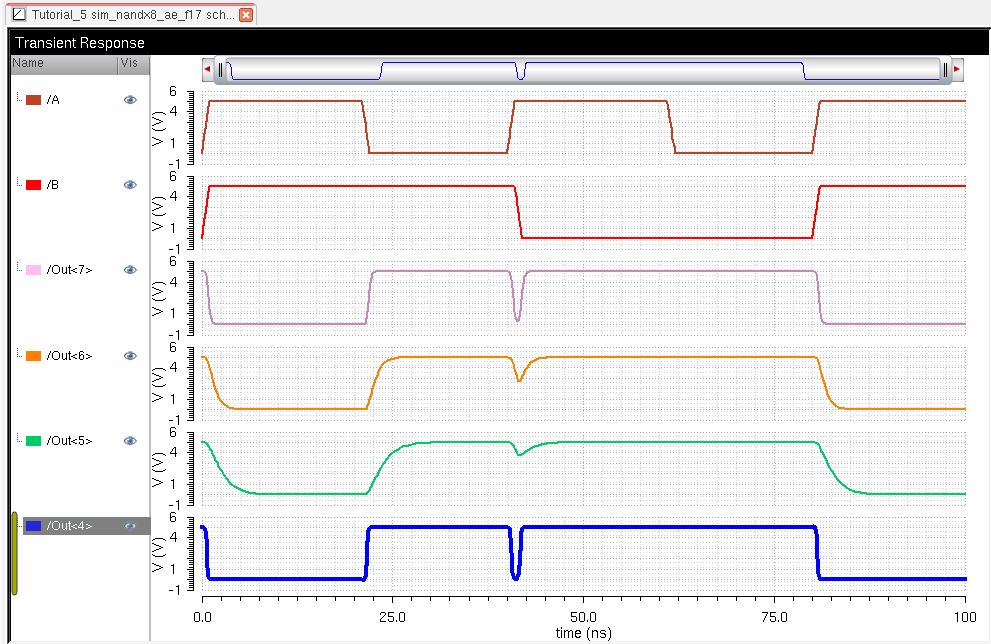
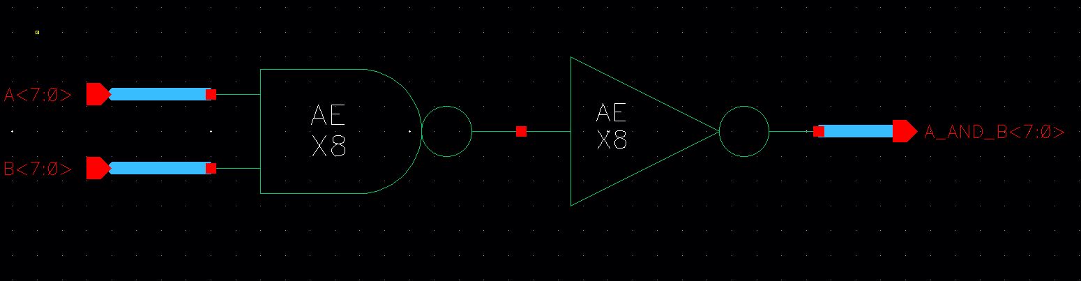
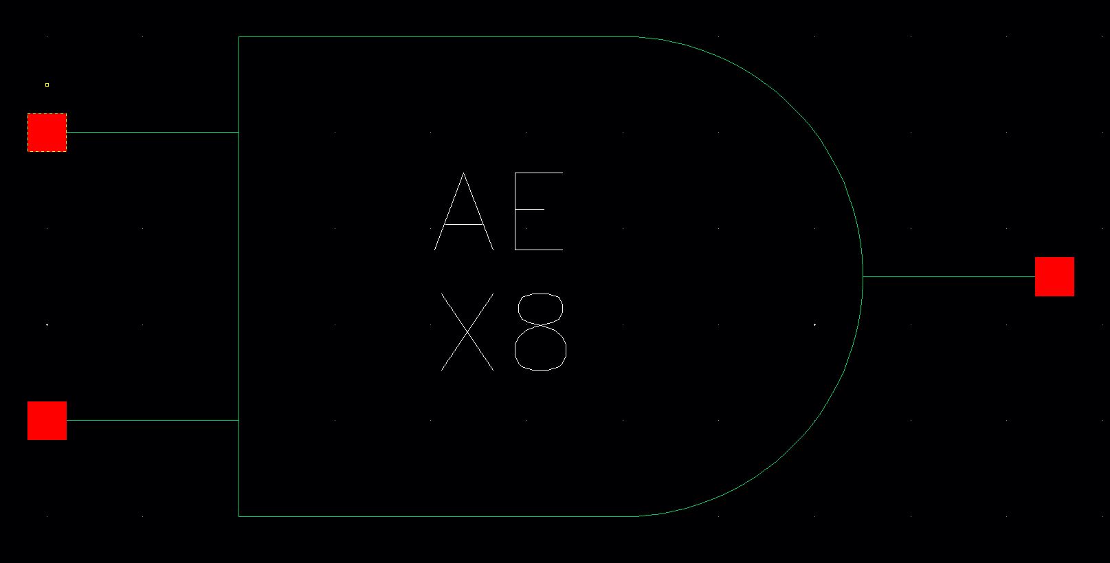
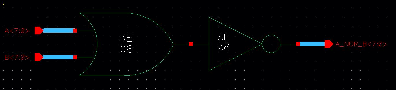
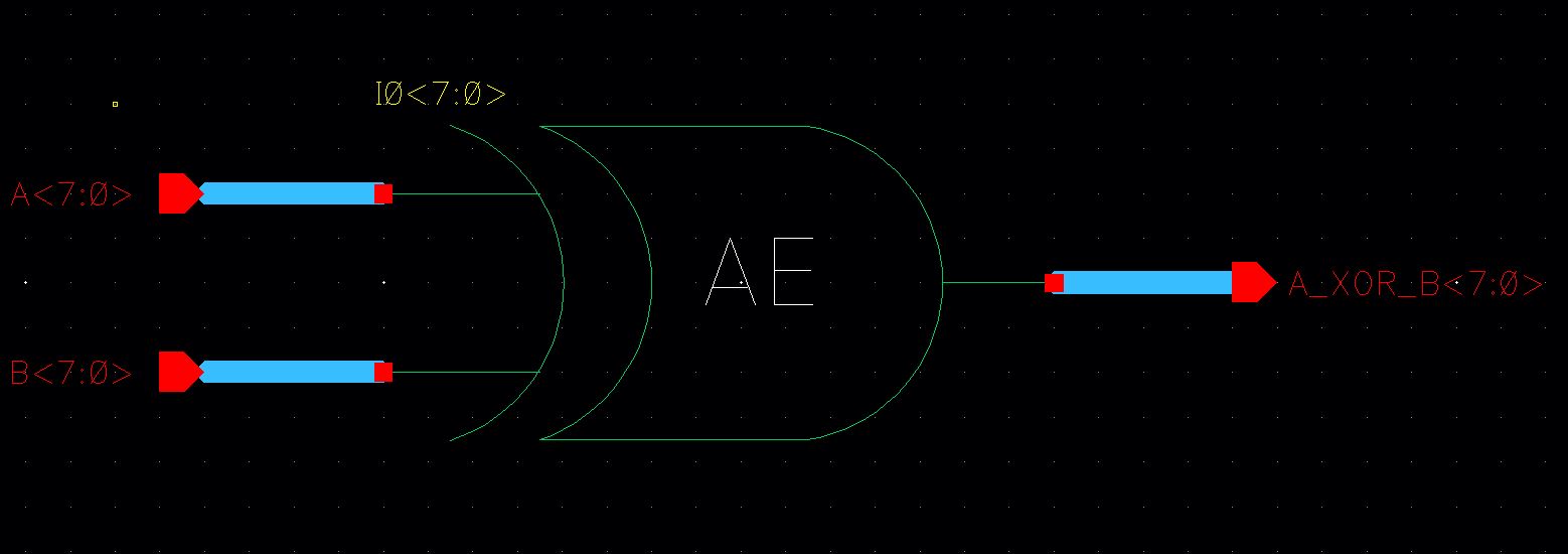
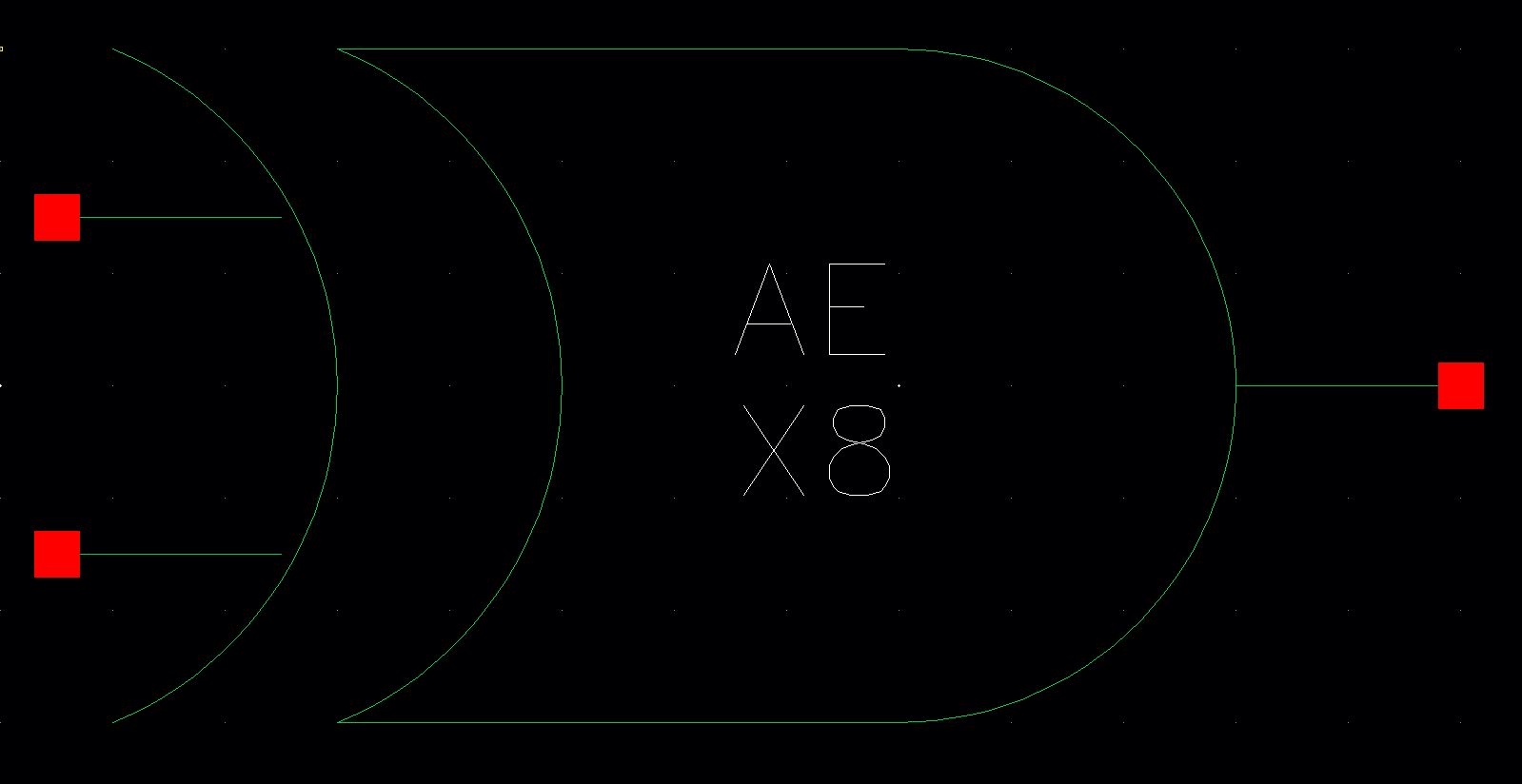
that we are familar with this process, we can do something similar to
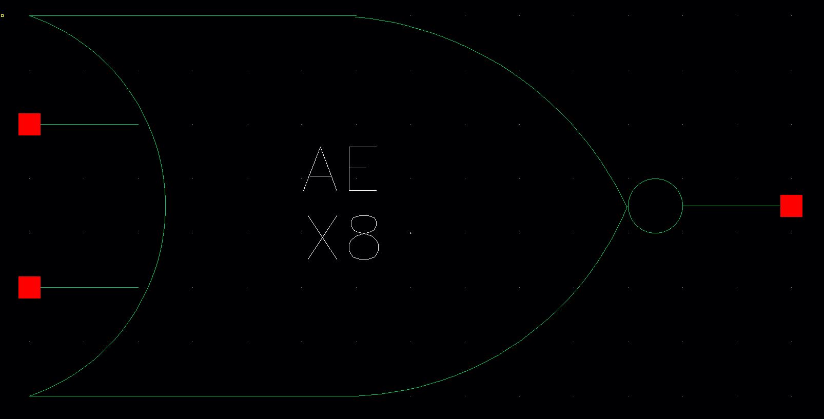
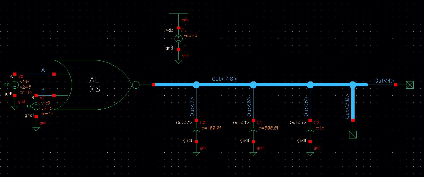
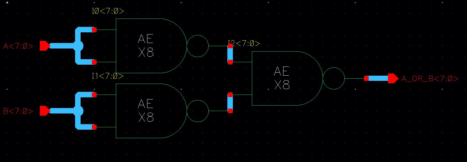
create an 8-bit version for an Inverter, NAND, AND, OR, XOR and NOR
logic gates
From
here, we are next asked to create a 2-to-1 demux/mux as well as an
8-bit version of the same schematic; here are the results of that
| Logic | Initial Schematic | Symbol | Simulation schematic | Results |
| 2-to-1 MUX | 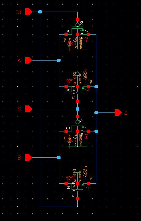 | 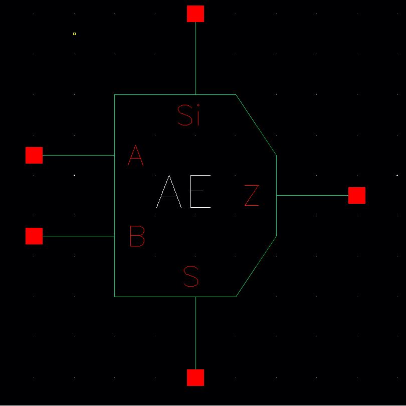 | 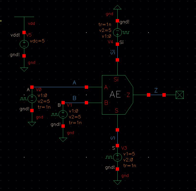 |  |
| 8 bit 2-to-1 MUX |  | 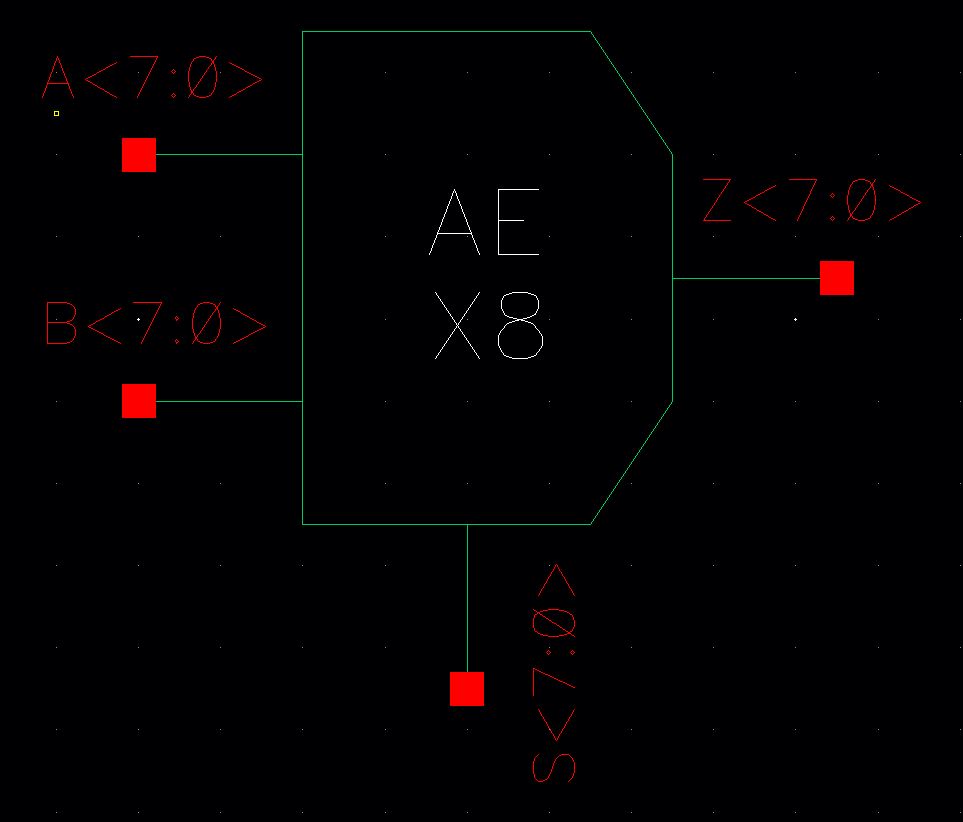 | 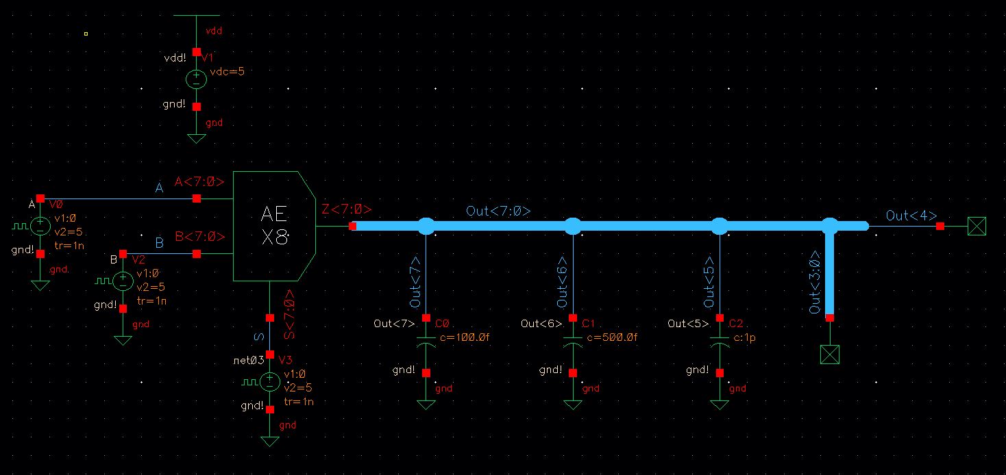 |  |
We
can sere by looking at the schematic the functions of this circuit. We
receive two inputs, A and B. but only 1 output. Which output is
selected is determined by the logic of the S or Si input. If S is high,
than the output is A, if Si is high (S is low) then the output is B.
This defines a 2-to-1 MUX.
Finally, we were asked to create a full adder and an 8-bit version of a full adder - this is now shown below.
| Logic | Initial Schematic | Symbol | Simulation schematic | Results |
| full adder | 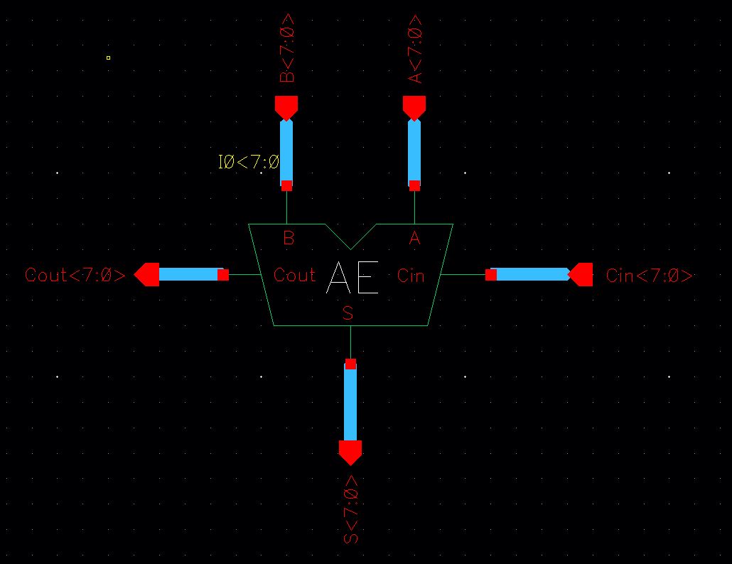 | 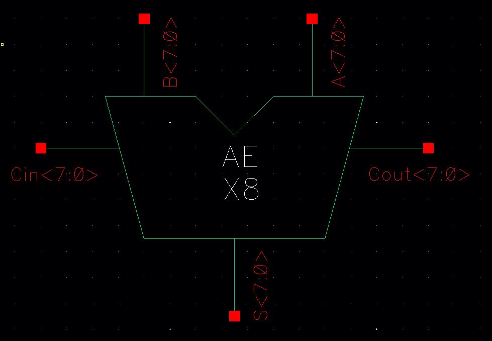 |  | 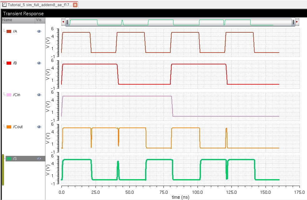 |
Here is my work backed up with a link to download and simulate all of these files
Link to backed up work
Return to Students
Return to EE 421L Labs


