Lab 04 - ECE 421L 

Authored by Aaron Escobedo

9/26/17


Prelab :: Follow the instructions and complete Tutorial 2

 Here is some of my data from Tutorial 2


                                                                            NMOS Transistor Data


http://cmosedu.com/jbaker/courses/ee421L/f17/students/escoba3/Lab4/Initial%20NMOS%20Transistor%20with%20pins.JPG
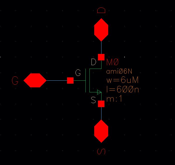
Initial NMOS Transistor Schematic
http://cmosedu.com/jbaker/courses/ee421L/f17/students/escoba3/Lab4/Initial%20NMOS%20Schematic%20Symbol.JPG
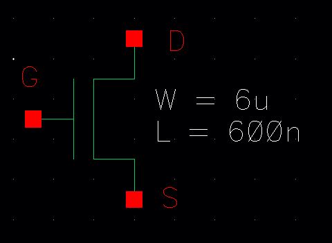
Initial Symbol View of NMOS Transistor
http://cmosedu.com/jbaker/courses/ee421L/f17/students/escoba3/Lab4/Initial%20Layout%20Design%20with%20pins.JPG
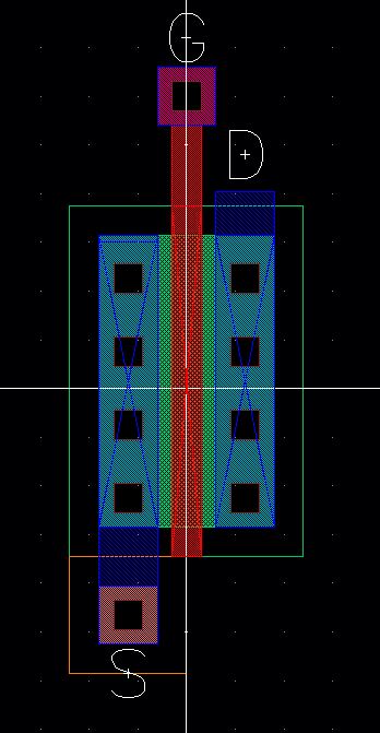
Initial Layout View of NMOS Transistor
http://cmosedu.com/jbaker/courses/ee421L/f17/students/escoba3/Lab4/Initial%20Layout%20Design%20(extracted).JPG
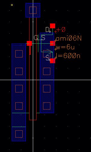
Initial Extracted View of NMOS Transistor


                                                                                                PMOS Transistor Data

http://cmosedu.com/jbaker/courses/ee421L/f17/students/escoba3/Lab4/Initial%20PMOS%20Schematic.JPG
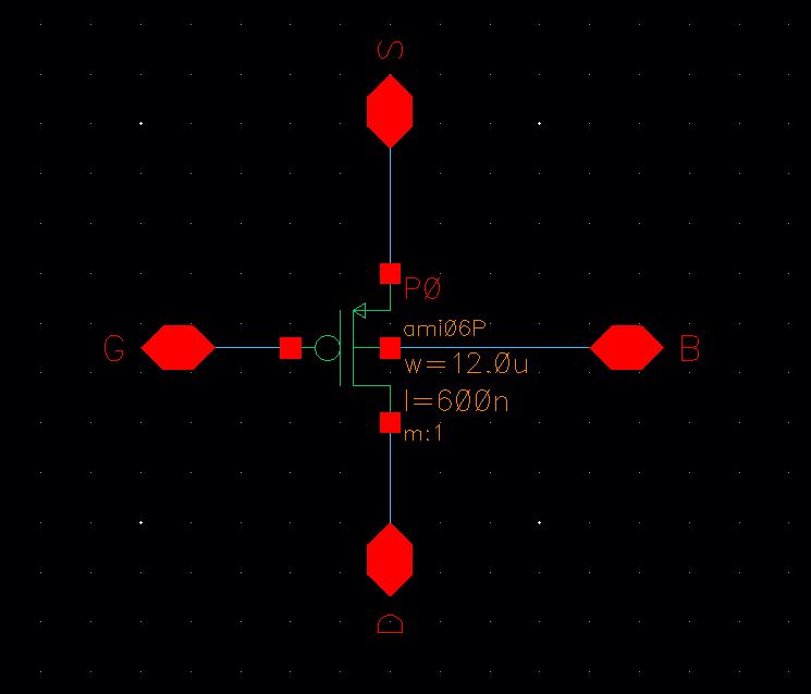
Initial PMOS Transistor Schematic
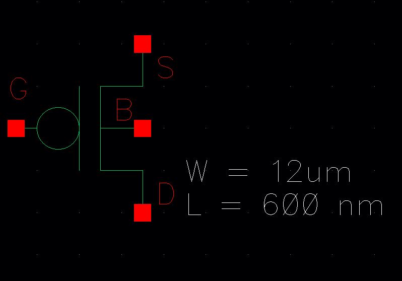
http://cmosedu.com/jbaker/courses/ee421L/f17/students/escoba3/Lab4/Initial%20PMOS%20Transistor.JPG
Initial Symbol View of PMOS Transistor
http://cmosedu.com/jbaker/courses/ee421L/f17/students/escoba3/Lab4/Initial%20PMOS%20Layout.JPG
Initial Layout View of PMOS Transistor
http://cmosedu.com/jbaker/courses/ee421L/f17/students/escoba3/Lab4/Initial%20PMOS%20Layout%20(extracted).JPG
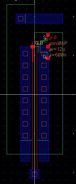
Initial Extracted View of PMOS Transistor

Lab Work

    - Generate 4 schematics and simulations

        1)
A schematic for simulating ID v. VDS of an NMOS device for VGS varying from 0 to 5 V in 1 V steps while VDS varies from 0 to 5 V in 1 mV steps. Use a 6u/600n width-to-length ratio.

http://cmosedu.com/jbaker/courses/ee421L/f17/students/escoba3/Lab4/Initial%20NMOS%20testing%20setup(2).JPG

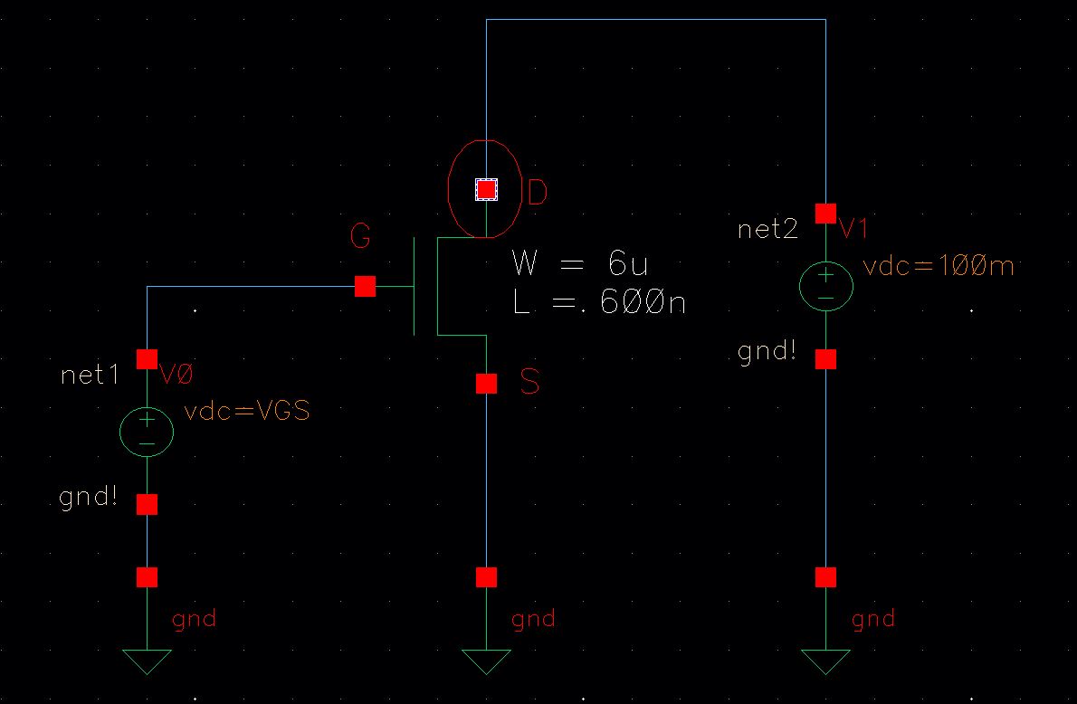
Initial NMOS transistor testing schematic
http://cmosedu.com/jbaker/courses/ee421L/f17/students/escoba3/Lab4/MOSFET%20IV%20Characteristics%20(extracted).JPG

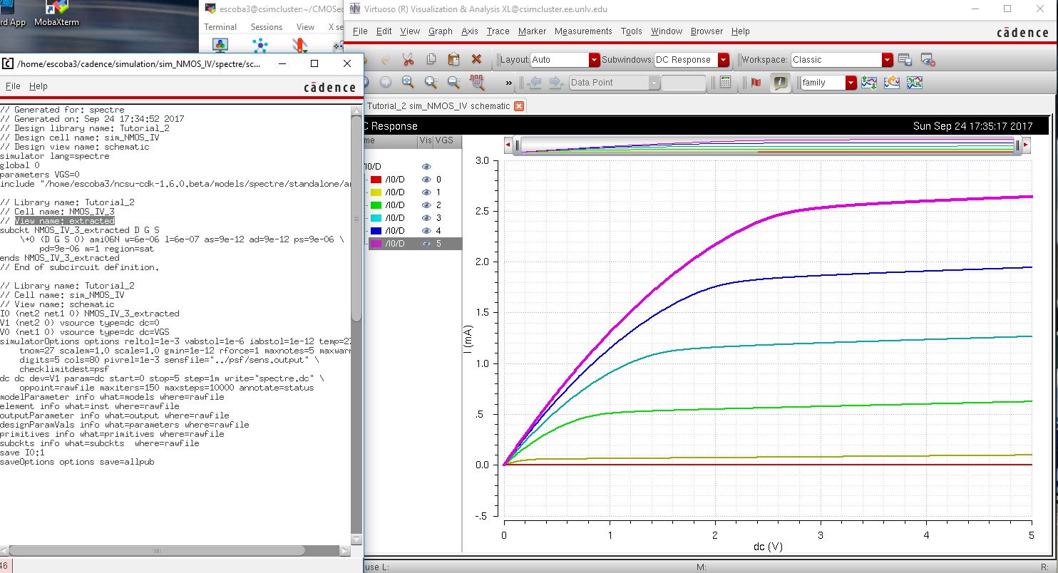
Results from Varying VGS from [0,5] with 1V steps


        2) A schematic for simulating ID v. VGS of an NMOS device for VDS = 100 mV where VGS varies from 0 to 2 V in 1 mV steps. Again use a 6u/600n width-to-length ratio.
     
http://cmosedu.com/jbaker/courses/ee421L/f17/students/escoba3/Lab4/Schematic%20for%20ID%20with%20VGS%20(0..2)%20VDS(100m).JPG
Setting up VDS = 100mV and Varying VGS from [0,2] in 1mV steps
http://cmosedu.com/jbaker/courses/ee421L/f17/students/escoba3/Lab4/Graph%20for%20ID%20with%20VGS%20(0..2)%20VDS(100m).JPG
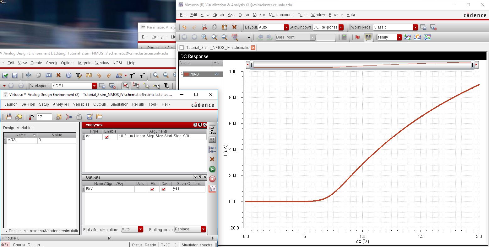
Results from said testing setup
     

        3) A schematic for simulating ID v. VSD of a PMOS device for VSG varying from 0 to 5 V in 1 V steps while VSD varies from 0 to 5 V in 1 mV steps. Use a 12u/600n width-to-length ratio.

http://cmosedu.com/jbaker/courses/ee421L/f17/students/escoba3/Lab4/Initial%20PMOS%20testing%20setup.JPG
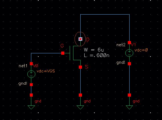
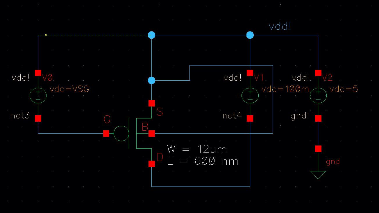
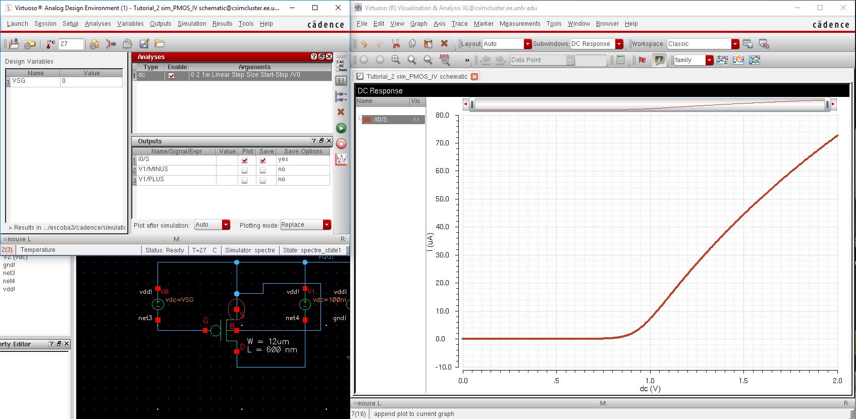
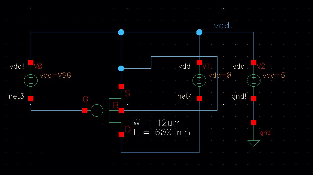
Initial PMOS transistor testing schematic
http://cmosedu.com/jbaker/courses/ee421L/f17/students/escoba3/Lab4/MOSFET%20IV%20PMOS%20Characteristics%20(extracted).JPG
Results from Varying VSG from [0,5] with 1V steps


        4) A schematic for simulating ID v. VSG of a PMOS device for VSD = 100 mV where VSG varies from 0 to 2 V in 1 mV steps. Again, use a 12u/600n width-to-length ratio.

http://cmosedu.com/jbaker/courses/ee421L/f17/students/escoba3/Lab4/Schematic%20for%20ID%20with%20VSG%20(0..2)%20VDS(100m)%20PMOS.JPGhttp://cmosedu.com/jbaker/courses/ee421L/f17/students/escoba3/Lab4/Graph%20for%20ID%20with%20VSG%20(0..2)%20VDS(100m)%20PMOS.JPG

    -
Lay out a 12u/0.6u PMOS device and connect all 4 MOSFET terminals to probe pads. 

http://cmosedu.com/jbaker/courses/ee421L/f17/students/escoba3/Lab4/Layout%20for%20PMOS%20with%20pads%20(DRC'ed).JPG
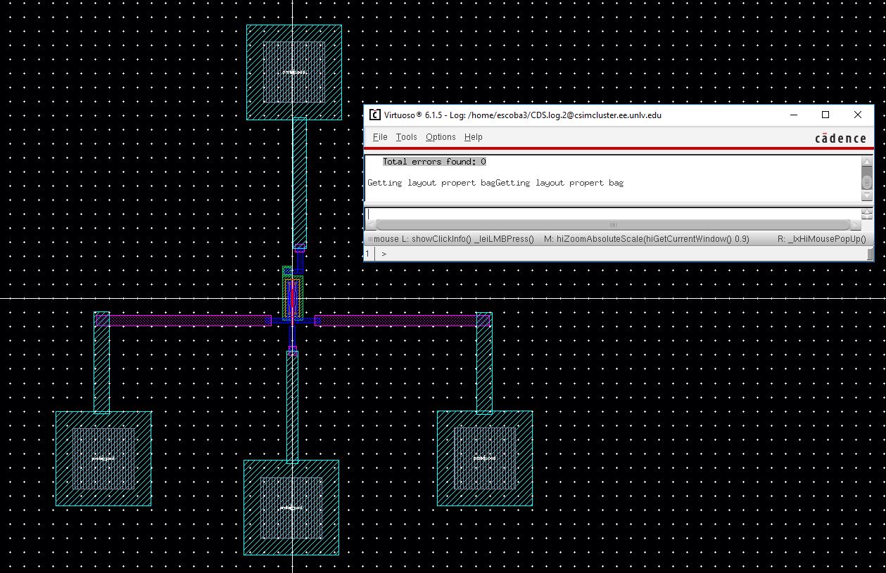
Layout Design with passed DRC
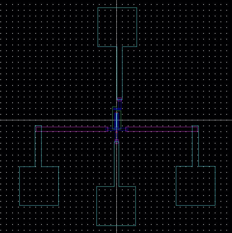
http://cmosedu.com/jbaker/courses/ee421L/f17/students/escoba3/Lab4/Layout%20for%20PMOS%20with%20pads%20(extracted).JPG
Extracted View of Layout
http://cmosedu.com/jbaker/courses/ee421L/f17/students/escoba3/Lab4/Layout%20for%20PMOS%20with%20pads%20(extracted,%20and%20zoomed)(.JPG
Extracted View focused on the PMOS


http://cmosedu.com/jbaker/courses/ee421L/f17/students/escoba3/Lab4/Schematic%20for%20PMOS%20With%20pads.JPG
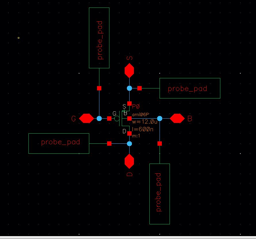
Corresponding Schematic for PMOS with pads
http://cmosedu.com/jbaker/courses/ee421L/f17/students/escoba3/Lab4/PMOS%20LVS%20Successful.JPG
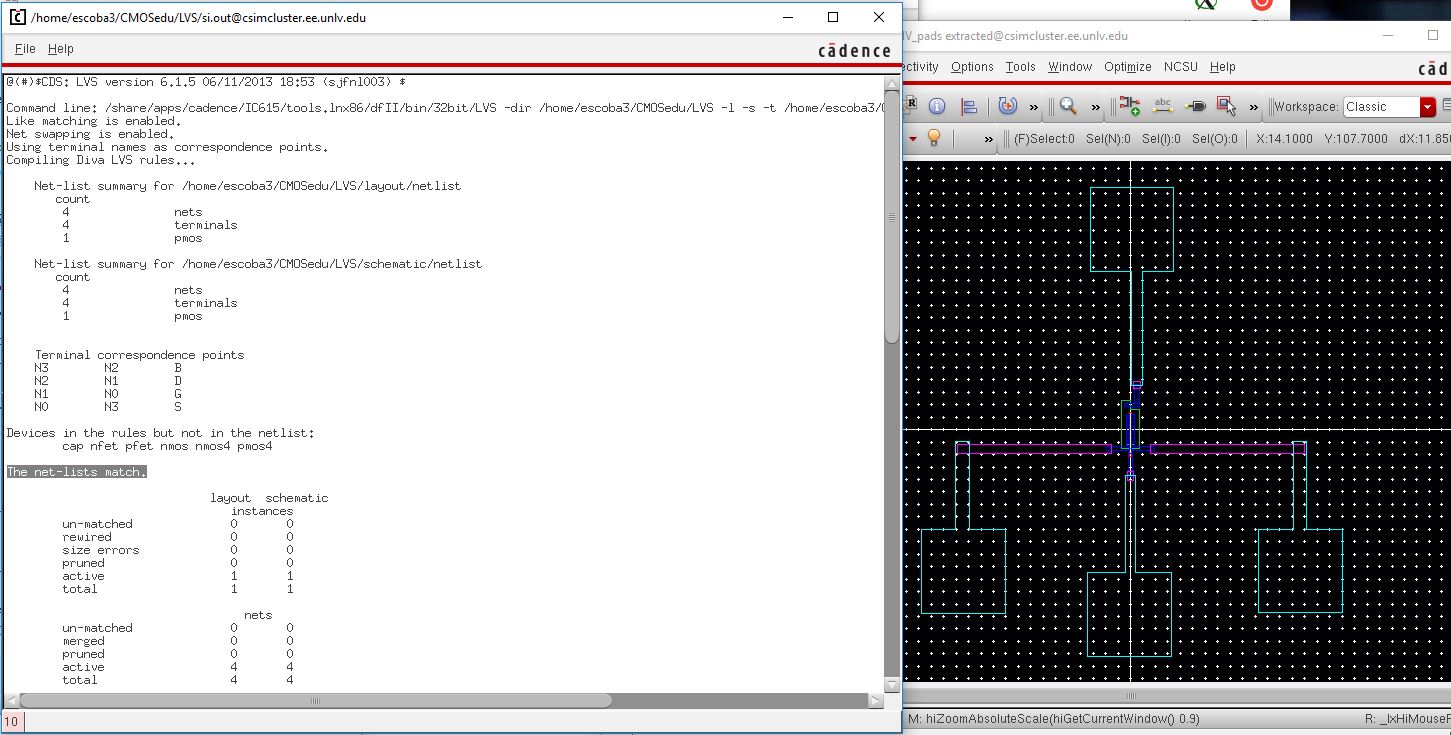
Results from LVS - Netlits match!


Return to Student Labs