Lab 7 -
EE 421L
Authored
by Reiner Dizon,
Email: dizonr1@unlv.nevada.edu
Today's
date is November 7, 2017
Lab
description: This
lab is about using buses and arrays for inverters, muxes, and adders.
PRELAB
- Back-up all of my work from the lab and the course
Lab Backup:
 | Course Backup:

|
I then ran
simulation on both schematics with initial conditions and models loaded in, and their simulations are identical.
I laid out the ring oscillator and DRCed it. Since the
schematic and layout were already created, I performed LVS afterwards to
confirm if the netlists matched.
Here is the schematic symbol for the ring oscillator:
Finally,
I ran the
simulation on both the schematic and the layout, and the simulations
were identical. For the simulating the NAND gate schematic, I created a
simulation schematic with power and ground.
Simulation Schematic:

Simulation Results (Schematic):

Simulation Results (Extracted):

- Read through the lab before starting
LAB
REPORT
1) Create a 4-bit Inverter
In
order to simplify circuit design for 4 inverters, I made a concise
schematic with the use of wide bus and instantiate an array of the
inverters. Here are my schematic and symbol:
Concise Schematic:

| Symbol:

|
I
simulated the inverters with different capacitive loads to observe the
rise and fall times. I observed that the delay increases as the
capacitance of the load increases. Here are my simulation schematic and waveform:Simulation Schematic:

| Simulation Waveform:

|
2) Create a 8-bit Inverter, NAND, XOR, AND, NOR, and OR gates
| Gate Name | Concise Schematic | Symbol | Simulation Waveform |
| NOT |  |  | 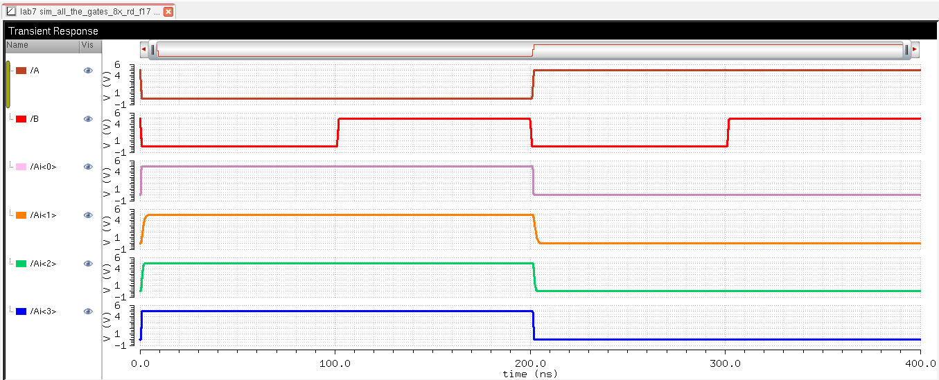 |
| NAND | 
| 
| 
|
| XOR | 
| 
| 
|
| AND | 
| 
| 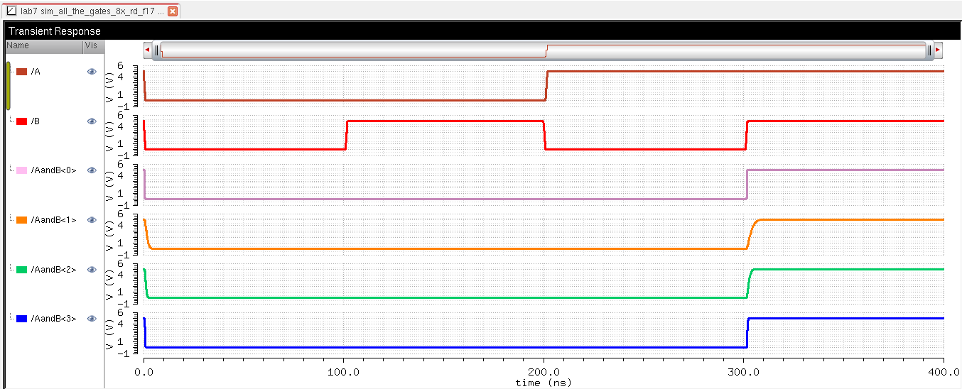
|
| NOR | 
| 
| 
|
| OR | 
| 
| 
|
Here is the simulation schematic for all of the simulations of all the gates:
3) Create a 2-to-1 DEMUX/MUX
Concise Schematic:

| Symbol:

|
Simulation Schematic:

| Simulation Waveform:

|
4) Create an 8-bit wide 2-to-1 DEMUX/MUX
Concise Schematic:

| Symbol:

|
Simulation Schematic:

| Simulation Waveform:

|
5) Create an 8-bit Full Adder
Concise Schematic:

| Symbol:

|
Layout (Full)
| 
|
Layout (Left)
| 
|
Layout (Right)
| 
|
DRC Results:

Extracted (Full)
| 
|
Extracted (Single)
| 
|
LVS Results:

Simulation Schematic:

Simulation Waveform (Schematic):

| Proof:

|
Simulation Waveform (Extracted):

| Proof:

|
After finishing the lab, I backed up my lab 7 web directory from CMOSedu and library from the cluster:

Return
to Reiner's Labs
Return
to EE 421L Labs


