Lab 5 -
EE 421L
Authored
by Reiner Dizon,
Email: dizonr1@unlv.nevada.edu
Today's
date is September 27, 2017
Lab
description: This
lab is about designing and laying out a CMOS inverter as well as simulating the design.
PRELAB
- Back-up all of your work from the lab and the course
Lab Backup:
 | Course Backup:

|
Schematic:

| Symbol:

|
Afterwards,
I created the layout for this particular inverter design. Since the
schematic and layout are then created, I performed an LVS afterwards to
confirm matching netlists.
Layout:

| LVS Results:

|
To
confirm the operation of both the schematic and the layout, a
simulation was ran on both designs, and the simulation was identical in
both. For the schematic, I created another simulation schematic.
Simulation Schematic:

| Simulation Results:

|
LAB
REPORT
1) Create schematic, symbol, and layout for 12u/6u (PMOS/NMOS ratio) inverter.
This
first inverter design is exactly the same from the design in the
tutorial. Thus, I copied the cell view from my prelab, so I can add
more to them. I slightly modified my schematic to make it more compact, and I added a text in the symbol which reads the
ratio "12u/6u" for this inverter.
Schematic:

| Symbol:

|
Since
I copied the entire cell view from my prelab (Tutorial 3), I only
modified the layout to add more contacts for the n-taps and p-taps
after editing the schematic and symbol. Instead of 2 contacts, there
are now 8 contacts for each taps, which decreases the resistance for
the interconnections among the layers. Here is my layout design and its
DRC results:
Layout:

| DRC Results:

|
After
performing DRC, I extracted the layout in order to perform LVS with the
schematic from earlier. Here is the extracted layout and the LVS
results:
Extracted:

| LVS Results:

|
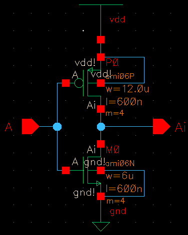
2) Create schematic, symbol, and layout for 48u/24u (PMOS/NMOS ratio) inverter (using a multiplier = 4).
This
other inverter design is a larger version of the previous inverter
design, but it uses the previous design nonetheless and applies a
multiplier of 4 to match the specifications. Hence, I copied the cell
view from the previous part to make changes. For each MOSFET, the width
and length is kept the same, but I added a multiplier of 4 for a ratio
of 48u/24u. Moreover, I added a text in the symbol "48u/24u" for this
inverter.
Schematic:

| Symbol:

|
Since
I copied the entire cell view from part 1, I have a template for the
bigger inverter since all of the necessary parts are there (i.e. ntaps,
ptaps, NMOS, PMOS, m1_poly). Just like the modifications that I made in
the schematic, I applied a multiplier of 4 for each transistor which
expanded their size. This increase means that I also expand the number
of contacts for each taps. Here is my layout design and its
DRC results:
Layout:

| DRC Results:

|
After
performing DRC, I extracted the layout in order to perform LVS with the
previous schematic. Here is the extracted layout and the LVS
results:
Extracted:

| LVS Results:

|
3) SPICE simulation of inverter circuit operation (driving capacitive loads of 100 fF, 1pF, 10pF, 100pF)
For
this part, I made two inverter schematic with a pulse signal that
drives a capacitive load of different capacitance for each inverter
type. To make simulation easier, I simply set the capacitance value of
the output capacitor to a design variable of COUT. With this
assignment, I could perform a parametric analysis onto the COUT
variable for the four capacitance values (mentioned above). Moreover,
for this part, I used Spectre for simulating each circuits. My
simulations show that as capacitance increase, the reaction at the
output (in terms of the falling edge) becomes less pronounced. This
relationship means that at higher capacitance the falling edge happens
much later and is less steep.
Part A: 12u/6u Inverter
Schematic:

Spectre Simulation:

Part B: 48u/24u Inverter
Schematic:

Spectre Simulation:

4) UltraSim simulation for same circuits of Part 3
For
these two simulations, I used the schematic from part 4 to perform the
UltraSim simulation onto with no changes. I simply made a new UltraSim
state for each corresponding schematic with the same settings as the
Spectre states in the previous part. With the simulations below, they
look extremely similar to the Spectre simulations from part 3 for each
inverter circuits. Because of this, the same relationship holds between
the capacitance and the reaction at the output where an increase in
capacitance leads to a slower reaction.
Part A: 12u/6u Inverter
UltraSim Simulation:

Part B: 48u/24u Inverter
UltraSim Simulation:

After finishing the lab, I backed up my lab 5 web directory from CMOSedu and library from the cluster:

Return
to Reiner's Labs
Return
to EE 421L Labs