Lab 07 - EE 421L 

Authored by Junho Bae

baej8@unlv.nevada.edu

November 8, 2017 


Pre-lab Work

Back-up all my work from this lab and the course.
Complete Tutorial 5.

In the tutorial, a 31 stage ring oscillator was designed.
The concept of labeling and incorporating buses to design concise schematics was practiced throughout this lab.

Lab Work
       
Drafting a 4-bit Inverter
     
Instead of making 4 separate inverters to invert a 4-bit word, I made an equivalent, more concise schematic.
By using an arrayed name, and connecting wide wires I drafted the concise schematic
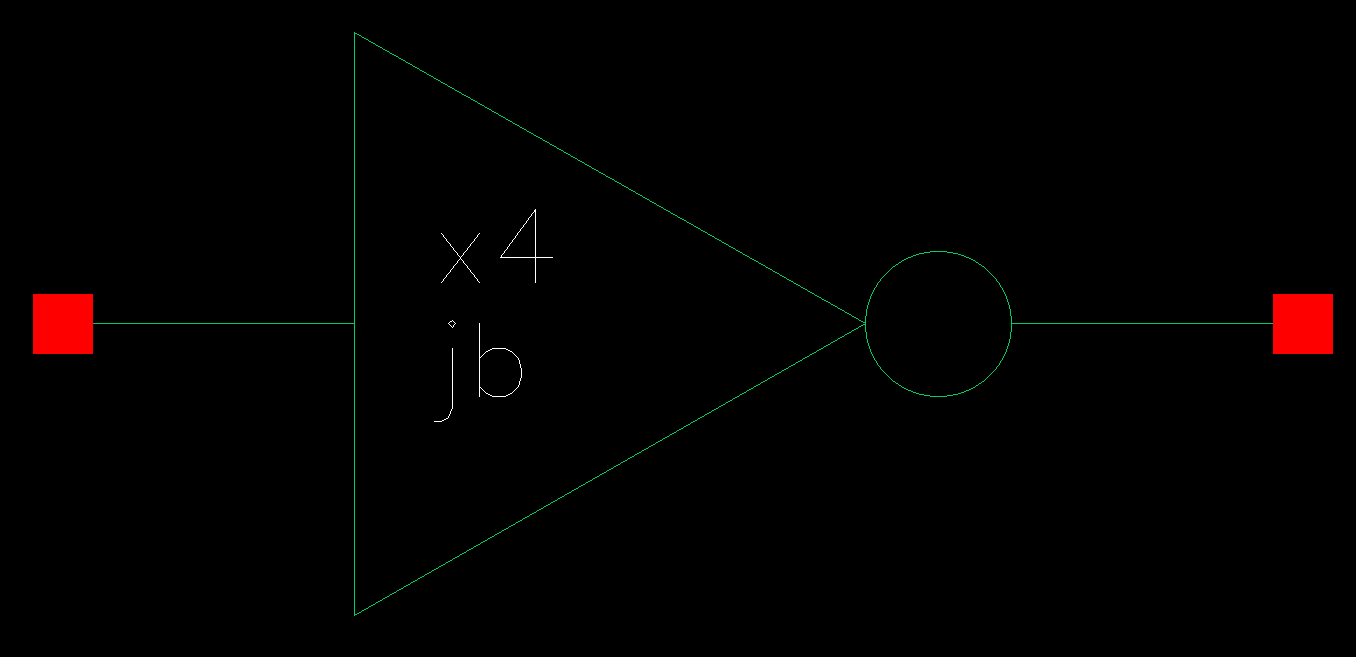
, and created a commonly used symbol. 
Transistor-level Schematic Concise Schematic Symbol
http://cmosedu.com/jbaker/courses/ee421L/f17/students/baej8/Lab%207/images/gates/1inv_schematic.PNGhttp://cmosedu.com/jbaker/courses/ee421L/f17/students/baej8/Lab%207/images/gates/4inv_schematic.PNGhttp://cmosedu.com/jbaker/courses/ee421L/f17/students/baej8/Lab%207/images/gates/4inv_symbol.PNG
     
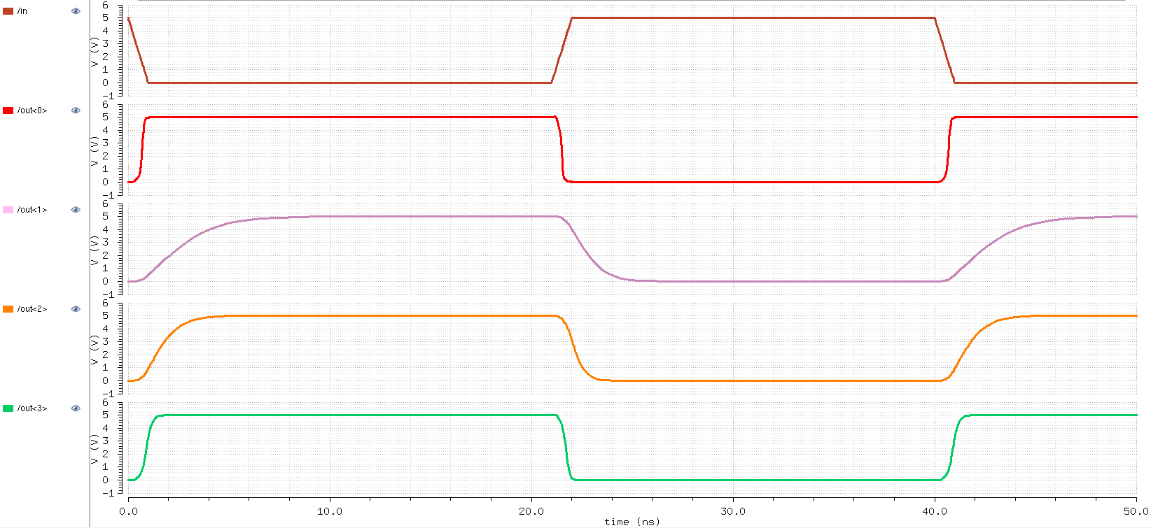
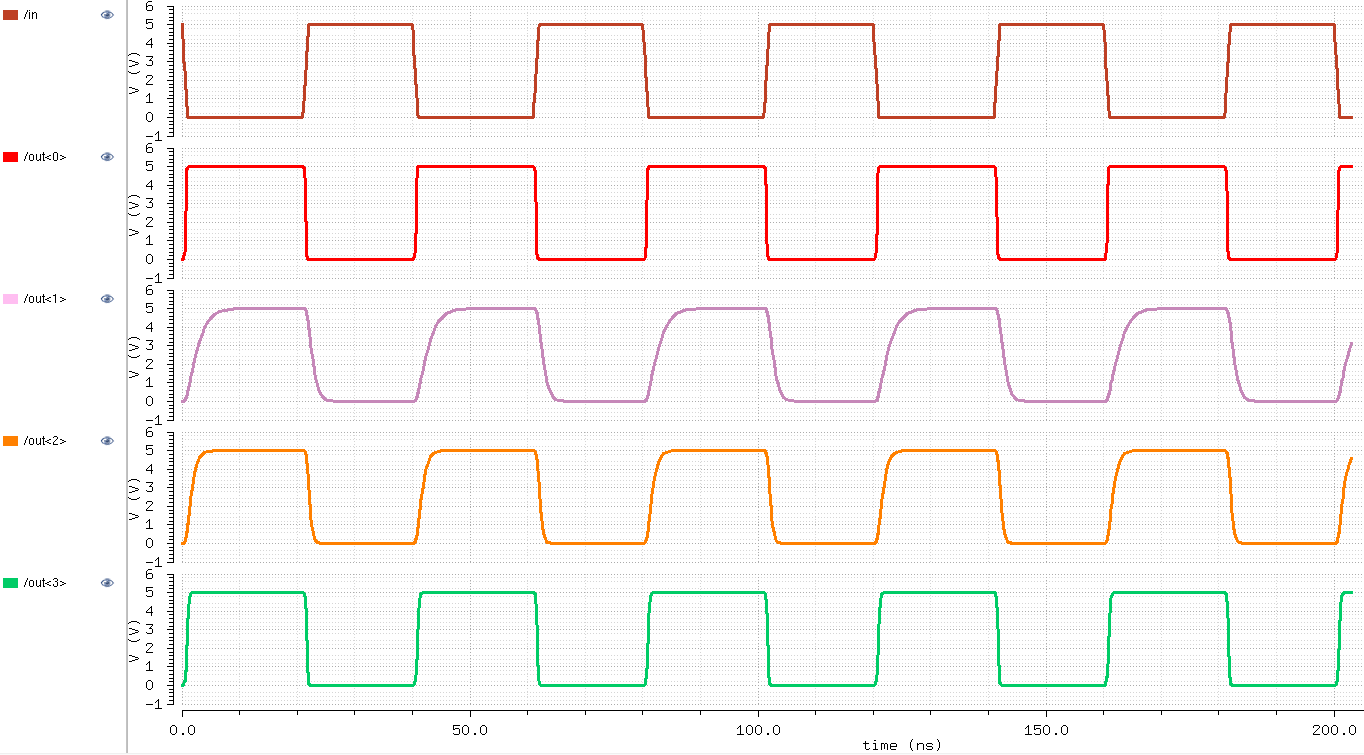
I tested out the 4-bit inverter by attaching different loads to see the rise/fall times of each output signal.
I noticed that the greater the capacitive load, the more influence it had on the inverted signal.
The rise and fall times increased as the capacitor values increased.  
Schematic of SimulationSimulation Result
http://cmosedu.com/jbaker/courses/ee421L/f17/students/baej8/Lab%207/images/gates/sim_4inv_schematic.PNGhttp://cmosedu.com/jbaker/courses/ee421L/f17/students/baej8/Lab%207/images/gates/sim_4inv_wave.PNG
       
Drafting 8-bit gates using 6u/0.6u MOSFETs
     
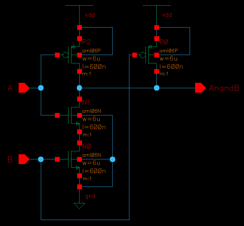
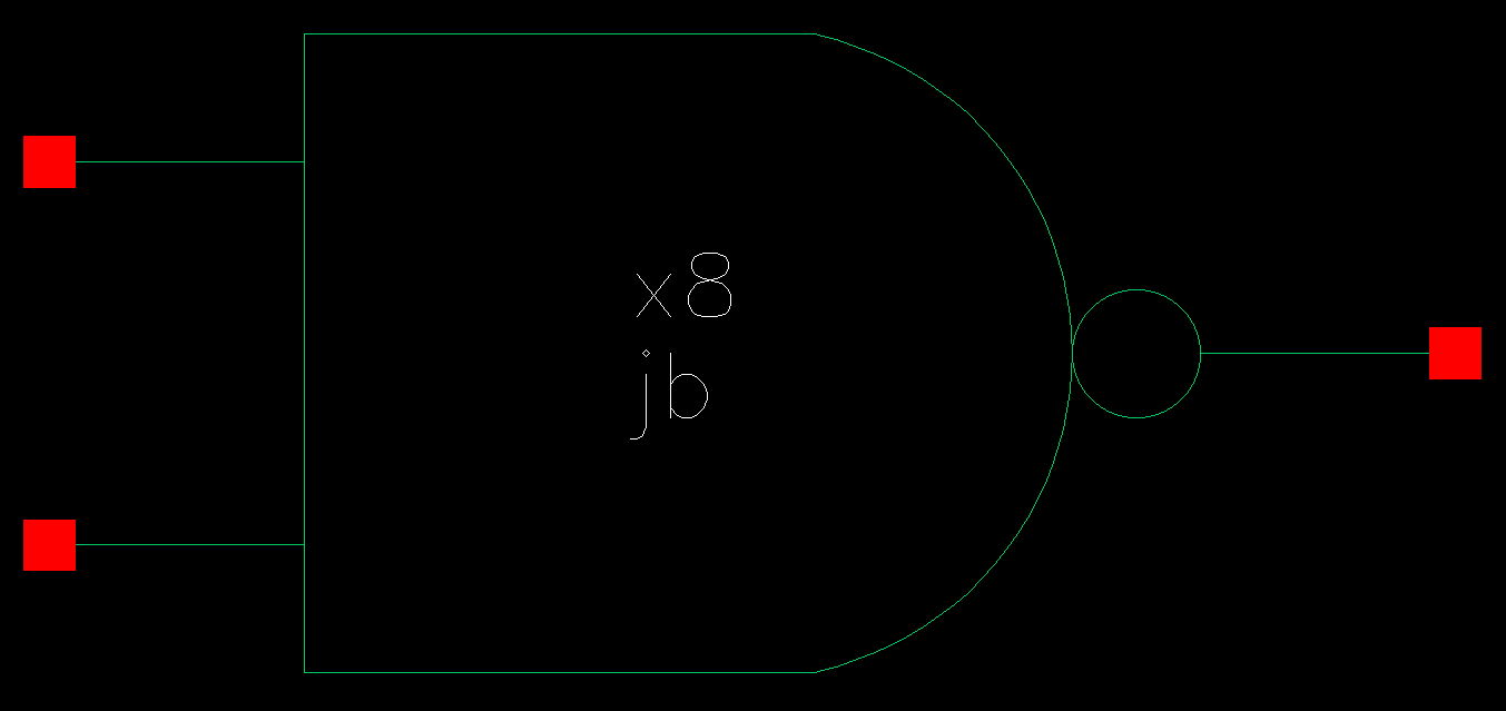
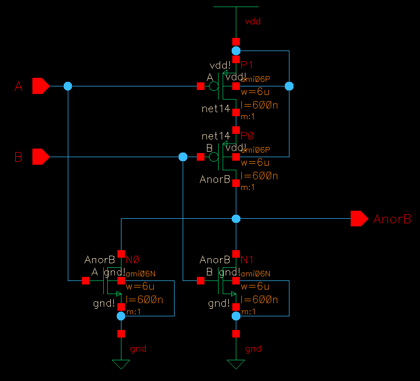
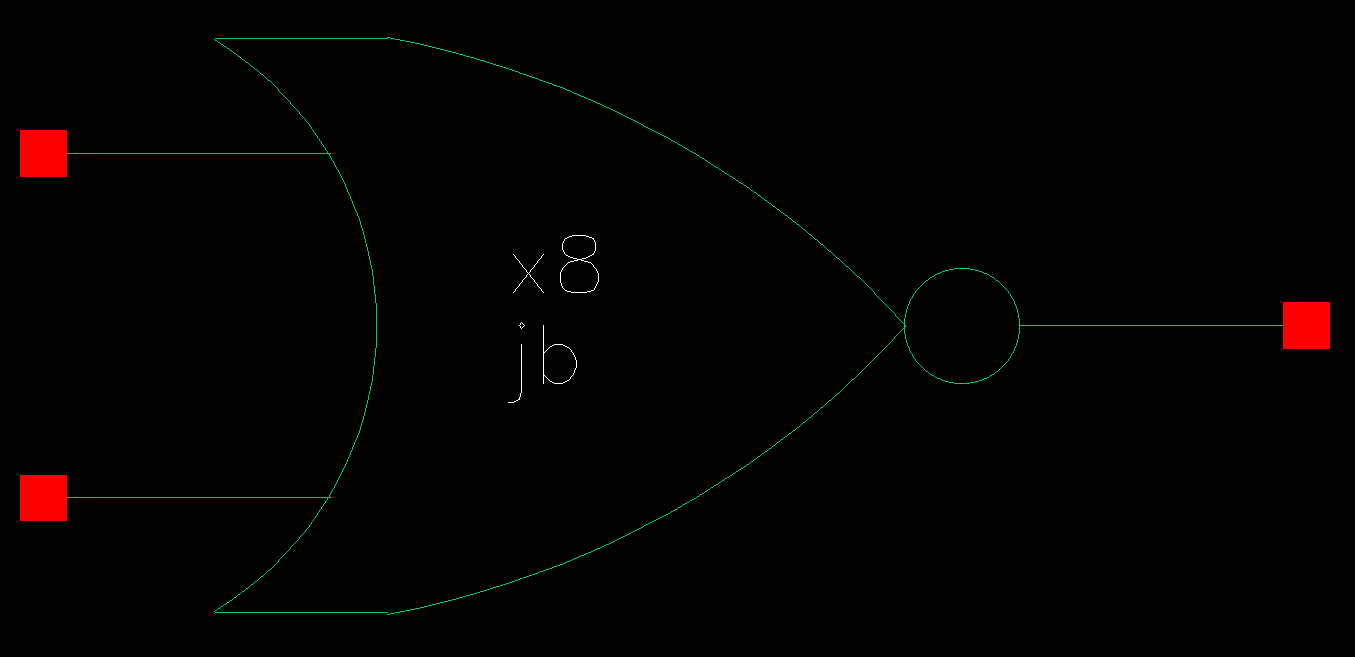
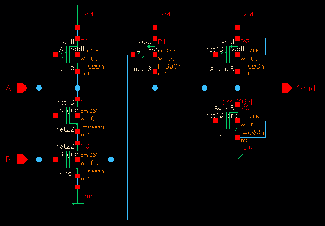
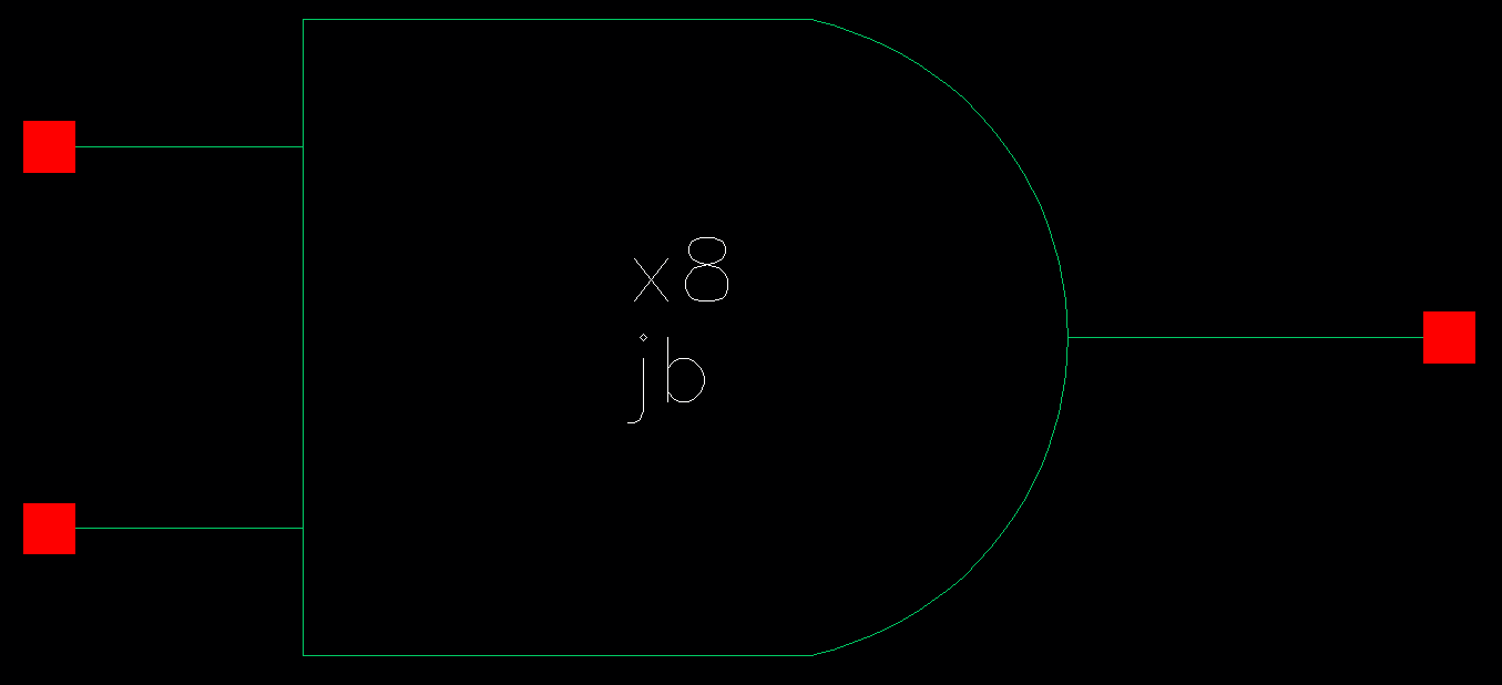
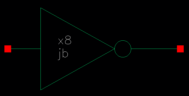
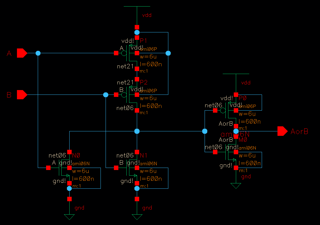
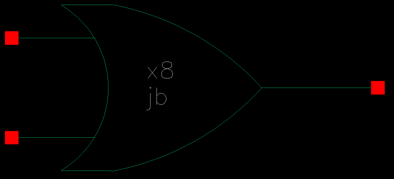
Applying the same concepts from the 4-bit invertor, I created schematics and symbols for 8 -bit input/output arrays of commonly used logic gates.
Logic GateTransistor-level Schematic Concise Schematic Symbol
NANDhttp://cmosedu.com/jbaker/courses/ee421L/f17/students/baej8/Lab%207/images/gates/1nand_schematic.PNGhttp://cmosedu.com/jbaker/courses/ee421L/f17/students/baej8/Lab%207/images/gates/8nand_schematic.PNGhttp://cmosedu.com/jbaker/courses/ee421L/f17/students/baej8/Lab%207/images/gates/8nand_symbol.PNG
NORhttp://cmosedu.com/jbaker/courses/ee421L/f17/students/baej8/Lab%207/images/gates/1nor_schematic.PNGhttp://cmosedu.com/jbaker/courses/ee421L/f17/students/baej8/Lab%207/images/gates/8nor_schematic.PNGhttp://cmosedu.com/jbaker/courses/ee421L/f17/students/baej8/Lab%207/images/gates/8nor_symbol.PNG
AND http://cmosedu.com/jbaker/courses/ee421L/f17/students/baej8/Lab%207/images/gates/1and_schematic.PNGhttp://cmosedu.com/jbaker/courses/ee421L/f17/students/baej8/Lab%207/images/gates/8and_schematic.PNGhttp://cmosedu.com/jbaker/courses/ee421L/f17/students/baej8/Lab%207/images/gates/8and_symbol.PNG
inverterhttp://cmosedu.com/jbaker/courses/ee421L/f17/students/baej8/Lab%207/images/gates/1inv_schematic.PNGhttp://cmosedu.com/jbaker/courses/ee421L/f17/students/baej8/Lab%207/images/gates/8inv_schematic.PNGhttp://cmosedu.com/jbaker/courses/ee421L/f17/students/baej8/Lab%207/images/gates/8inv_symbol.PNG
ORhttp://cmosedu.com/jbaker/courses/ee421L/f17/students/baej8/Lab%207/images/gates/1or_schematic.PNGhttp://cmosedu.com/jbaker/courses/ee421L/f17/students/baej8/Lab%207/images/gates/8or_schematic.PNGhttp://cmosedu.com/jbaker/courses/ee421L/f17/students/baej8/Lab%207/images/gates/8or_schematic.PNGhttp://cmosedu.com/jbaker/courses/ee421L/f17/students/baej8/Lab%207/images/gates/8or_symbol.PNG
       
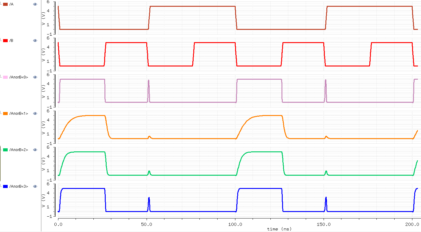
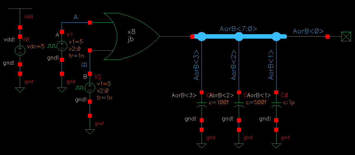
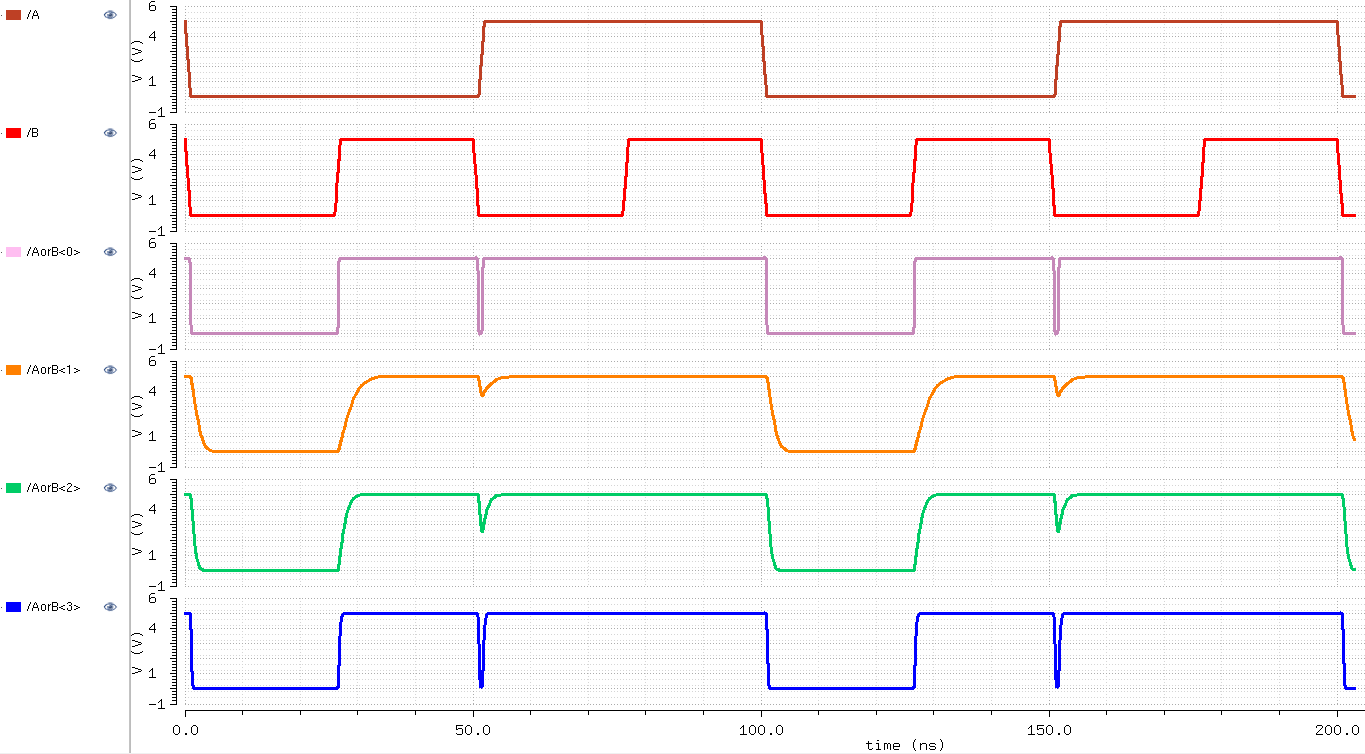
I simulated the the 8-bit gates and observed similar patterns with different loads.
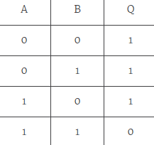
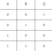
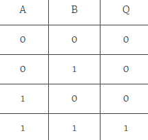
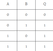
I made sure that the results matched the truth tables of each gate.
Logic GateSchematic of SimulationSimulation ResultTruth Table
NANDhttp://cmosedu.com/jbaker/courses/ee421L/f17/students/baej8/Lab%207/images/gates/sim_8nand_schematic.PNGhttp://cmosedu.com/jbaker/courses/ee421L/f17/students/baej8/Lab%207/images/gates/sim_8nand_wave.PNG
http://cmosedu.com/jbaker/courses/ee421L/f17/students/baej8/Lab%207/images/gates/nand.PNG
NORhttp://cmosedu.com/jbaker/courses/ee421L/f17/students/baej8/Lab%207/images/gates/sim_8nor_schematic.PNGhttp://cmosedu.com/jbaker/courses/ee421L/f17/students/baej8/Lab%207/images/gates/sim_8nor_wave.PNGhttp://cmosedu.com/jbaker/courses/ee421L/f17/students/baej8/Lab%207/images/gates/nor.PNG
AND http://cmosedu.com/jbaker/courses/ee421L/f17/students/baej8/Lab%207/images/gates/sim_8and_schematic.PNGhttp://cmosedu.com/jbaker/courses/ee421L/f17/students/baej8/Lab%207/images/gates/sim_8and_wave.PNGhttp://cmosedu.com/jbaker/courses/ee421L/f17/students/baej8/Lab%207/images/gates/and.PNG
inverterhttp://cmosedu.com/jbaker/courses/ee421L/f17/students/baej8/Lab%207/images/gates/sim_8inv_schematic.PNGhttp://cmosedu.com/jbaker/courses/ee421L/f17/students/baej8/Lab%207/images/gates/sim_8inv_wave.PNG
http://cmosedu.com/jbaker/courses/ee421L/f17/students/baej8/Lab%207/images/gates/not.PNG
ORhttp://cmosedu.com/jbaker/courses/ee421L/f17/students/baej8/Lab%207/images/gates/sim_8or_schematic.PNGhttp://cmosedu.com/jbaker/courses/ee421L/f17/students/baej8/Lab%207/images/gates/sim_8or_wave.PNGhttp://cmosedu.com/jbaker/courses/ee421L/f17/students/baej8/Lab%207/images/gates/or.PNGhttp://cmosedu.com/jbaker/courses/ee421L/f17/students/baej8/Lab%207/images/gates/or.PNG
       
Drafting a 2-to-1 DEMUX/MUX
   
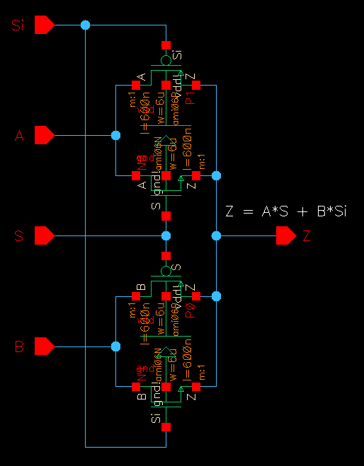
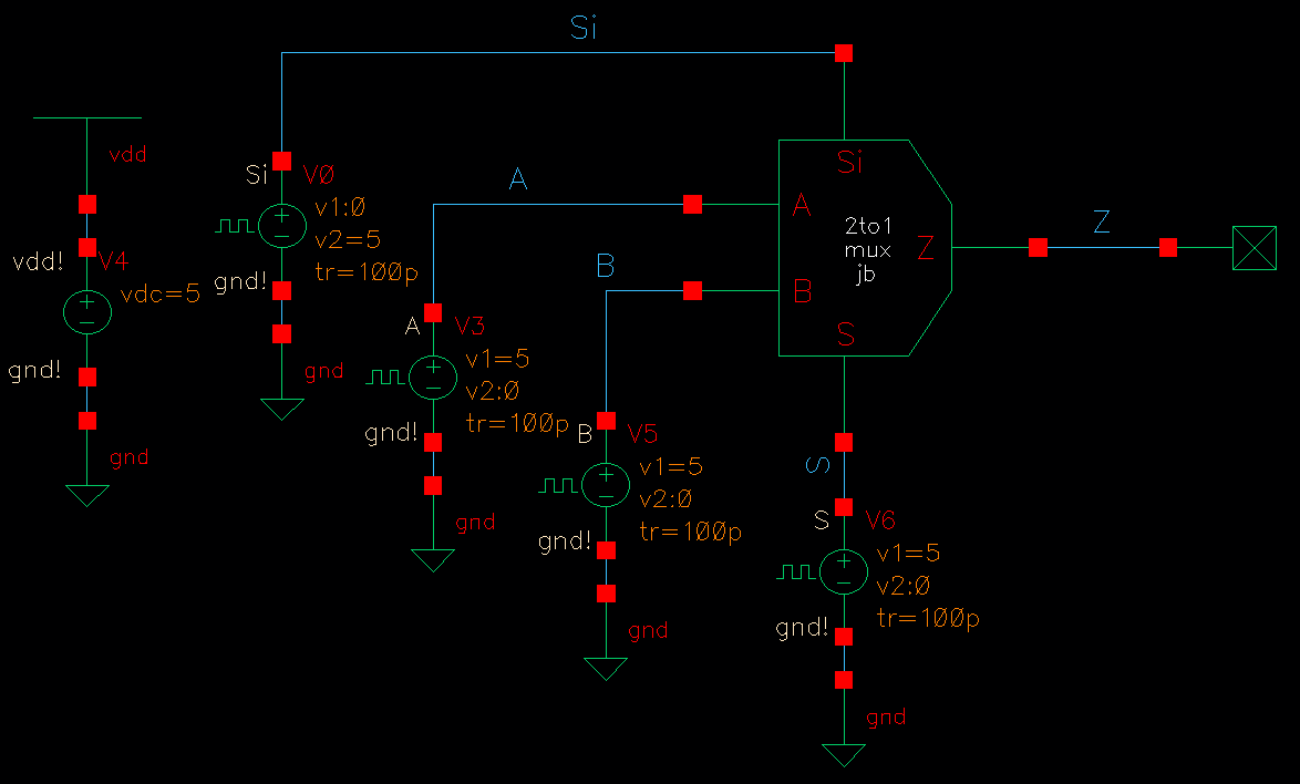
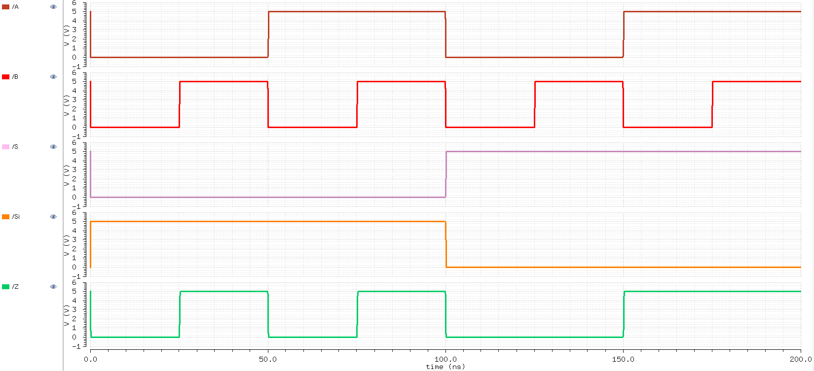
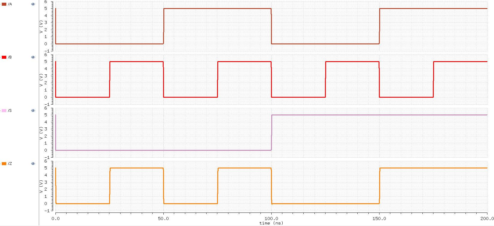
I created a schematic of a 2-to-1 multiplexer where the output was dependent on the control signal 'S'.
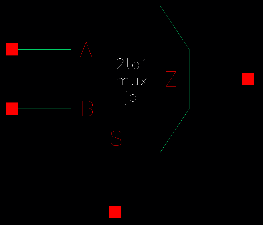
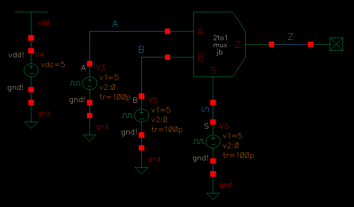
I created a symbol, and simulated the schematic with all possible combination of input signals.
As the simulation shows, when S is high, and S' is low, the output echoed the input 'B' signal, and
when S was low and S' was high, the output echoed the input 'A' signal
Transistor-level Schematic  Symbol2-to-1 MUX Simulation SchematicSimulation Result
http://cmosedu.com/jbaker/courses/ee421L/f17/students/baej8/Lab%207/images/mux/1mux_schematic.PNG
http://cmosedu.com/jbaker/courses/ee421L/f17/students/baej8/Lab%207/images/mux/1mux_symbol.PNG
http://cmosedu.com/jbaker/courses/ee421L/f17/students/baej8/Lab%207/images/mux/sim_1mux_schematic.PNGhttp://cmosedu.com/jbaker/courses/ee421L/f17/students/baej8/Lab%207/images/mux/sim_1mux_wave.PNG
   
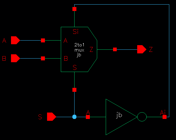
An inverter was include in my design so that only one select signal was needed.
The simulation was the same as the MUX from above with only 1 select input, 'S'.
SchematicSymbol2-to-1 MUX Simulation SchematicSimulation Result
http://cmosedu.com/jbaker/courses/ee421L/f17/students/baej8/Lab%207/images/mux/mux_inv_schematic.PNGhttp://cmosedu.com/jbaker/courses/ee421L/f17/students/baej8/Lab%207/images/mux/mux_inv_symbol.PNGhttp://cmosedu.com/jbaker/courses/ee421L/f17/students/baej8/Lab%207/images/mux/sim_muxinv_schematic.PNGhttp://cmosedu.com/jbaker/courses/ee421L/f17/students/baej8/Lab%207/images/mux/sim_muxinv_wave.PNG
   
Drafting an 8-bit 2-to-1 DEMUX/MUX
   
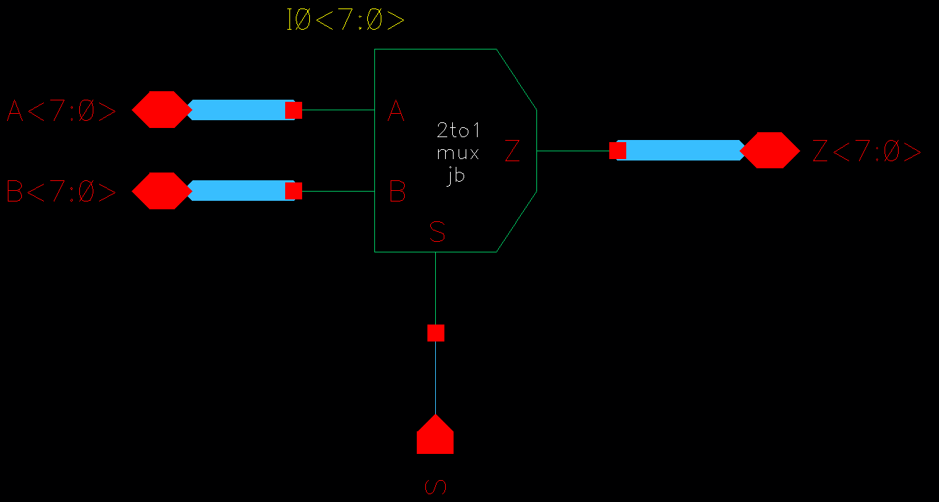
By instantiating a single 2-to-1 MUX, I created an 8-bit 2-to-1 MUX using buses.
Schematic Symbol
http://cmosedu.com/jbaker/courses/ee421L/f17/students/baej8/Lab%207/images/mux/8mux_schematic.PNG
http://cmosedu.com/jbaker/courses/ee421L/f17/students/baej8/Lab%207/images/mux/8mux_symbol.PNG
   
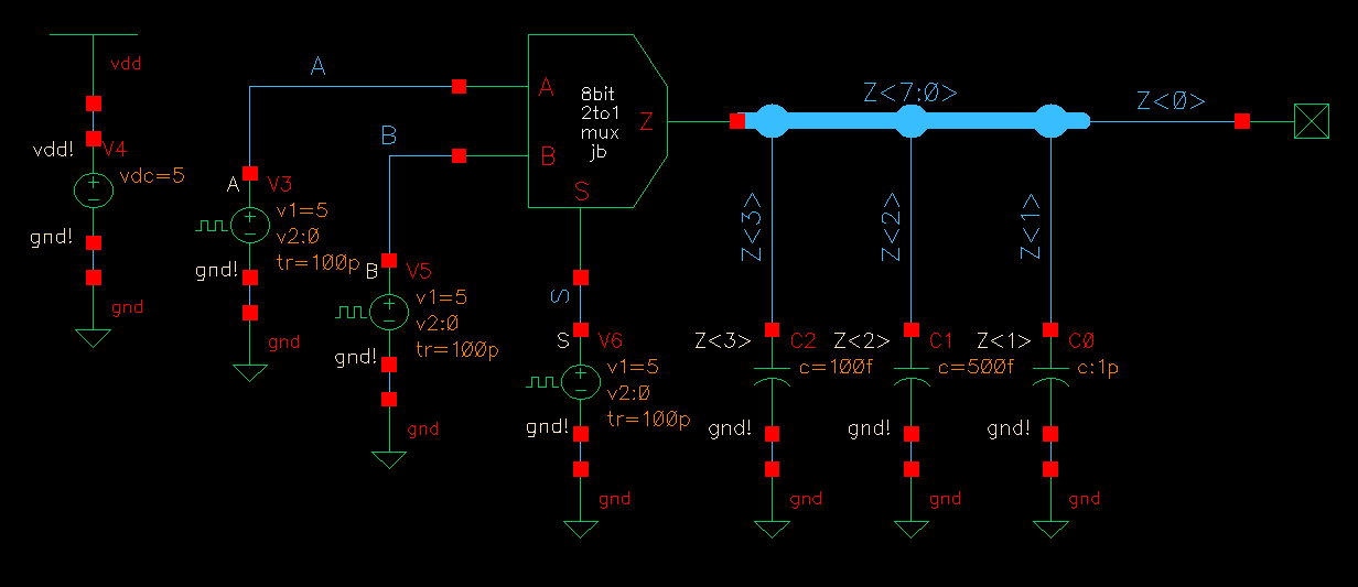
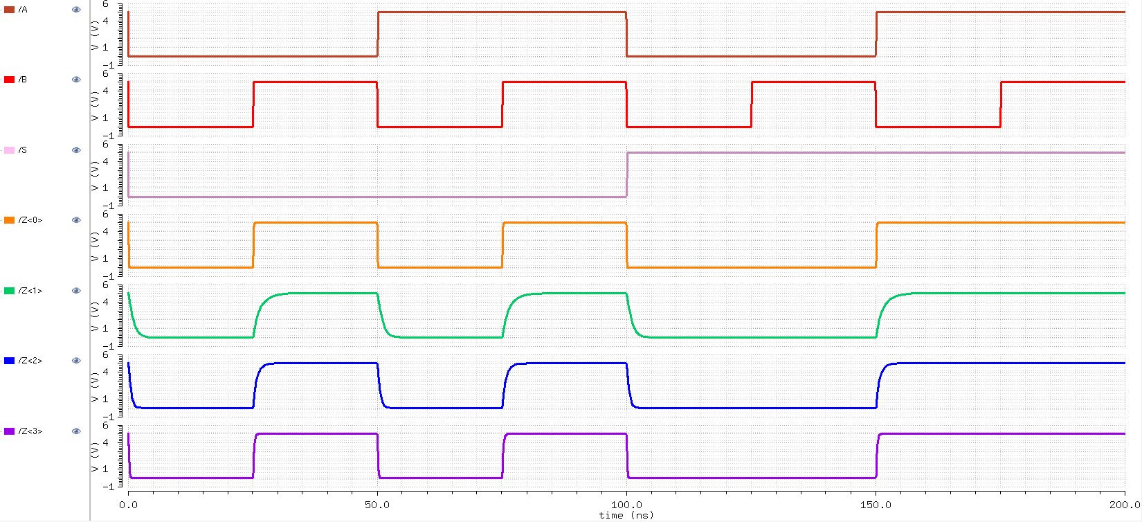
Again, I simulated the schematic to see if the MUX was working properly.
2-to-1 MUX Simulation SchematicSimulation Result
http://cmosedu.com/jbaker/courses/ee421L/f17/students/baej8/Lab%207/images/mux/sim_8mux_schematic.PNGhttp://cmosedu.com/jbaker/courses/ee421L/f17/students/baej8/Lab%207/images/mux/sim_8mux_wave.PNG
   
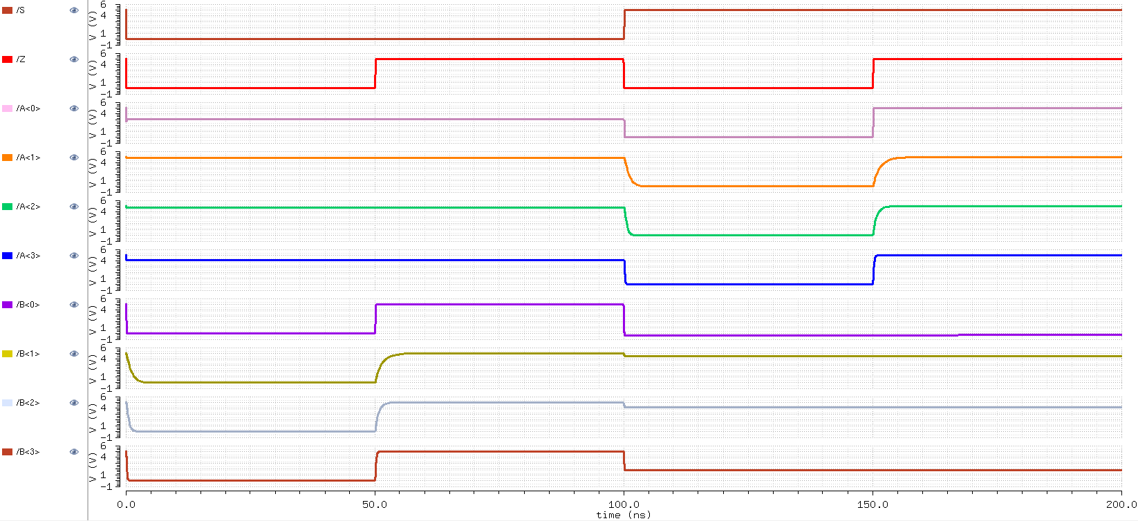
The input signals replicated by pulse sources in the schematic below, were attached to the Z and S pin to test out the circuits de-multiplexing functionality.
The signal fed into the Z terminal was seen on the A terminal when the control signal 'S' was high,
and was seen on the B terminal when the control signal 'S' was low.
2-to-1 DEMUX Simulation SchematicSimulation Result
http://cmosedu.com/jbaker/courses/ee421L/f17/students/baej8/Lab%207/images/mux/sim_8demux_schematic.PNGhttp://cmosedu.com/jbaker/courses/ee421L/f17/students/baej8/Lab%207/images/mux/sim_8demux_wave.PNG
     
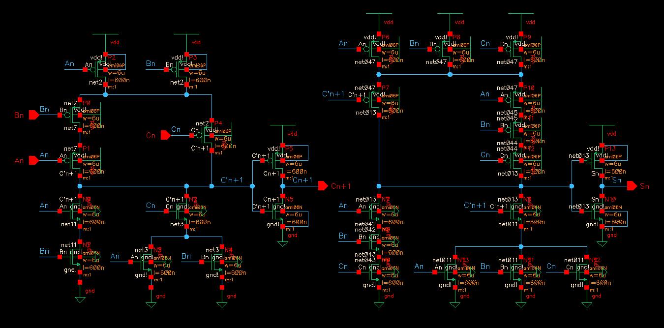
Drafting the Full Adder seen in Fig. 12.20
   
AOI implementation of a full adder
   
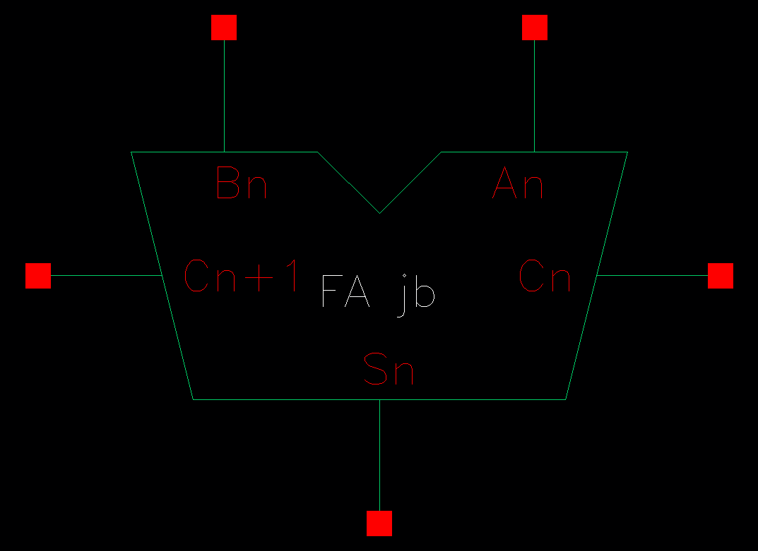
I created the schematic of a high-speed adder and made an adder symbol for the circuit.  
Transistor-level Schematic  Symbol
http://cmosedu.com/jbaker/courses/ee421L/f17/students/baej8/Lab%207/images/8adder/x1fa_schematic.PNG
http://cmosedu.com/jbaker/courses/ee421L/f17/students/baej8/Lab%207/images/8adder/x1fa_symbol.PNG
     
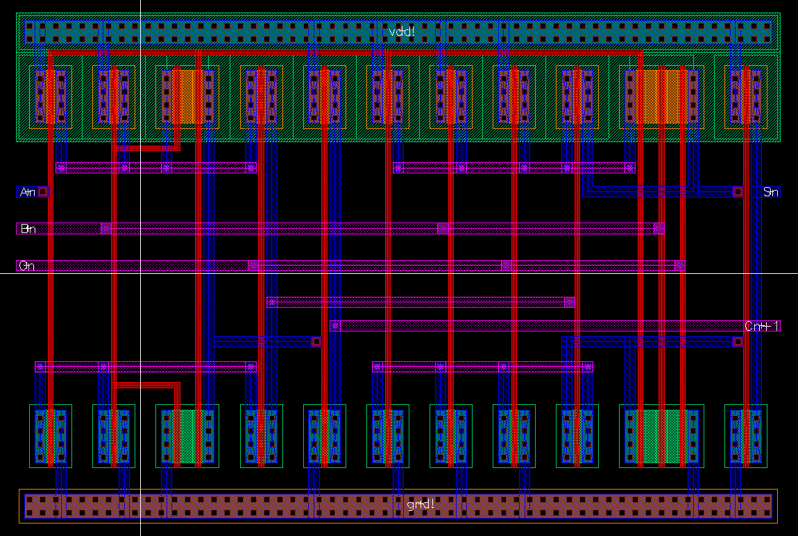
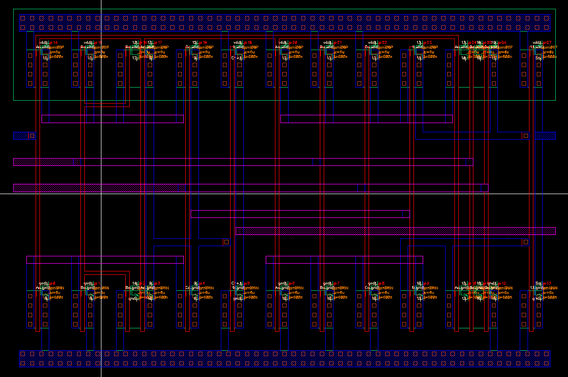
Below are images of the layout and extracted views of the full adder.
I made sure the inputs and outputs of the full-adder were routed to metal1 or metal2.
LayoutExtracted
http://cmosedu.com/jbaker/courses/ee421L/f17/students/baej8/Lab%207/images/8adder/x1fa_layout.PNGhttp://cmosedu.com/jbaker/courses/ee421L/f17/students/baej8/Lab%207/images/8adder/x1fa_extracted.PNG
   
DRC successful
http://cmosedu.com/jbaker/courses/ee421L/f17/students/baej8/Lab%207/images/8adder/x1fa_drc.PNG
   
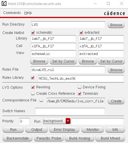
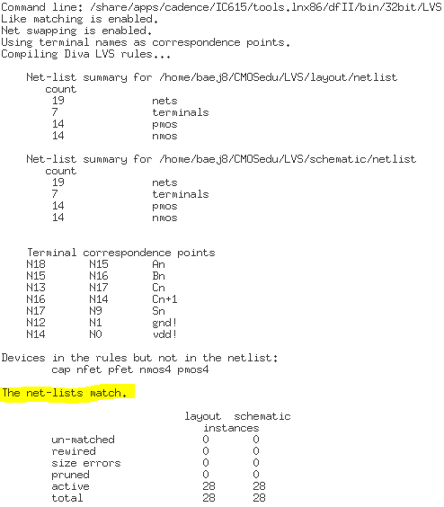
LVS successful
http://cmosedu.com/jbaker/courses/ee421L/f17/students/baej8/Lab%207/images/8adder/x1fa_lvs.PNG
http://cmosedu.com/jbaker/courses/ee421L/f17/students/baej8/Lab%207/images/8adder/x1fa_lvs_out.PNG
   
Full-Adder Simulations
   
Once the the Layout and Schematic matched, I proceeded to simulated the full adder.
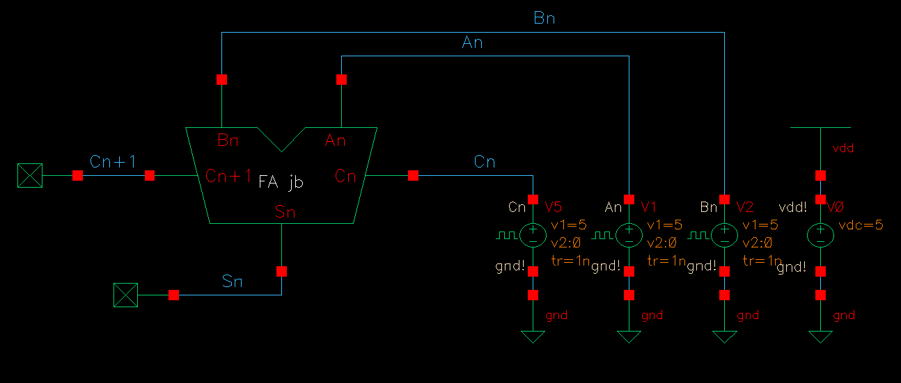
Below are the simulation results of both the layout and the schematic.
Simulation Schematic
http://cmosedu.com/jbaker/courses/ee421L/f17/students/baej8/Lab%207/images/8adder/sim_x1fa_schematic.PNG
   
Simulation Netlist Simulation Result
http://cmosedu.com/jbaker/courses/ee421L/f17/students/baej8/Lab%207/images/8adder/sim_x1fa_schematic_netlist.PNG
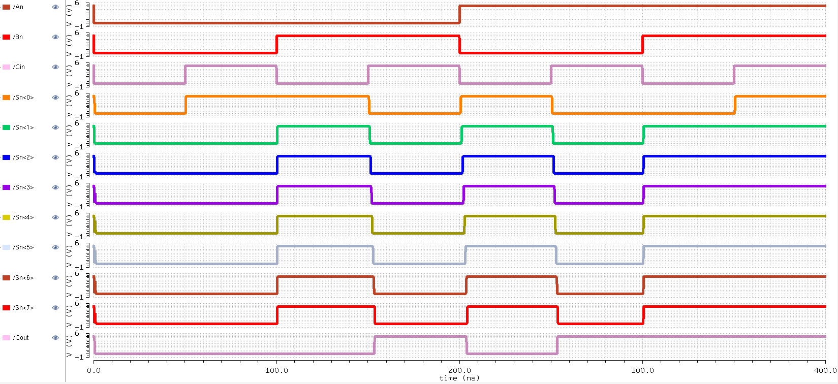
http://cmosedu.com/jbaker/courses/ee421L/f17/students/baej8/Lab%207/images/8adder/sim_x1fa_schematic_wave.PNG
http://cmosedu.com/jbaker/courses/ee421L/f17/students/baej8/Lab%207/images/8adder/sim_x1fa_extracted_netlist.PNG
http://cmosedu.com/jbaker/courses/ee421L/f17/students/baej8/Lab%207/images/8adder/sim_x1fa_extracted_wave.PNG
   
Full-Adder Truth Table
a b cin s cout
0 0 0 0 0
0 0 1 1 0
0 1 0 1 0
0 1 1 0 1
1 0 0 1 0
1 0 1 0 1
1 1 0 0 1
1 1 1 1 1
       
I didn't notice any differences between the extracted and schematic simulations.
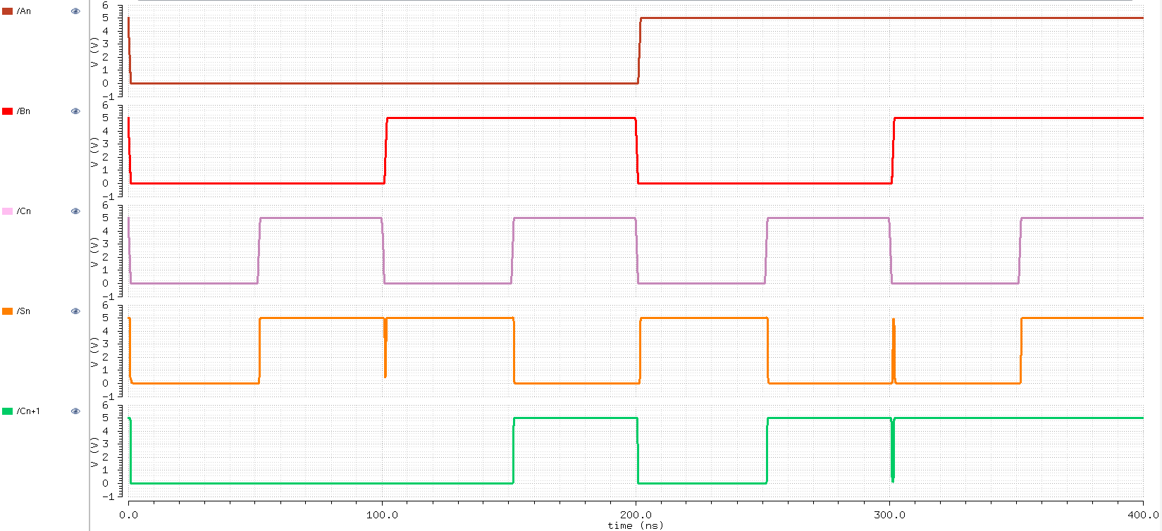
The simulation results matched the truth table of a logical full adder; however the glitches persisted.
When more than 1 input signal was changing simultaneously, the output signal was not clear.
   
Drafting an 8-bit High-Speed Adder
   
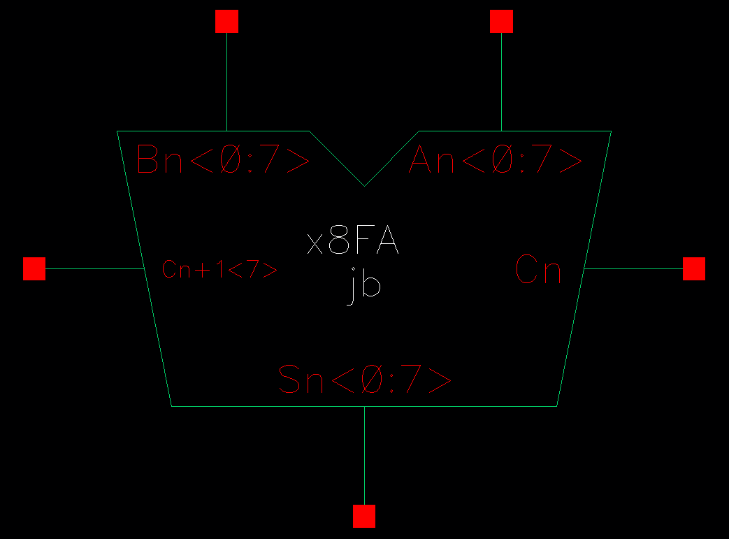
I instantiated the full adder from above to create an 8-bit adder using wire buses and arrayed names.
The first carry-out bit was fed into the carry-in terminal of the next full-adder and so forth. 
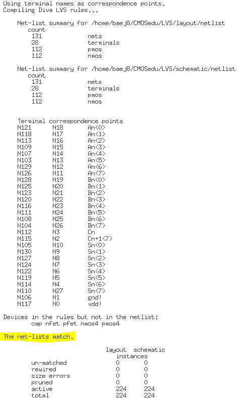
Following the layout and extracted images are successful LVS and DRC images.
   
Schematic Symbol
http://cmosedu.com/jbaker/courses/ee421L/f17/students/baej8/Lab%207/images/8adder/x8fa_schematic.PNG
http://cmosedu.com/jbaker/courses/ee421L/f17/students/baej8/Lab%207/images/8adder/x8fa_symbol.PNG
   
Below are images of the layout and extracted views of the 8-bit adder.
Layout http://cmosedu.com/jbaker/courses/ee421L/f17/students/baej8/Lab%207/images/8adder/x8fa_layout.PNG
Extracted http://cmosedu.com/jbaker/courses/ee421L/f17/students/baej8/Lab%207/images/8adder/x8fa_extracted.PNG
   
DRC successful
http://cmosedu.com/jbaker/courses/ee421L/f17/students/baej8/Lab%207/images/8adder/x8fa_drc.PNG
   
LVS successful
http://cmosedu.com/jbaker/courses/ee421L/f17/students/baej8/Lab%207/images/8adder/x8fa_lvs.PNG
http://cmosedu.com/jbaker/courses/ee421L/f17/students/baej8/Lab%207/images/8adder/x8fa_lvs_out.PNG
   
8-bit Adder Simulations
   
Once the the Layout and Schematic matched, I proceeded to simulated the 8-bit adder.
Below are the simulation results of both the layout and the schematic.
Simulation Schematic
http://cmosedu.com/jbaker/courses/ee421L/f17/students/baej8/Lab%207/images/8adder/sim_x8fa_schematic.PNG
   
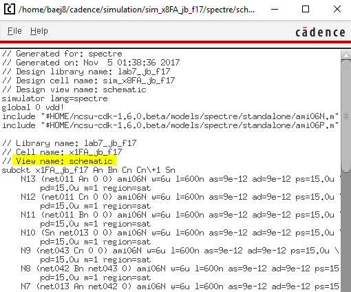
Similar to the full adder simulations, I didn't notice anything different between the two different simulations.
Simulation Netlist Simulation Result
http://cmosedu.com/jbaker/courses/ee421L/f17/students/baej8/Lab%207/images/8adder/sim_x8fa_schematic_netlist.PNG
http://cmosedu.com/jbaker/courses/ee421L/f17/students/baej8/Lab%207/images/8adder/sim_x8fa_schematic_wave.PNG
http://cmosedu.com/jbaker/courses/ee421L/f17/students/baej8/Lab%207/images/8adder/sim_x8fa_extracted_netlist.PNG
http://cmosedu.com/jbaker/courses/ee421L/f17/students/baej8/Lab%207/images/8adder/sim_x8fa_extracted_wave.PNG
   
Final design directory: lab7_jb.zip
     

Return to Junho's Labs

Return to EE421L Labs