Lab 06 -
EE 421L
Authored
by Junho Bae
baej8@unlv.nevada.edu
October 25, 2017
Pre-lab
work
Back-up all my work from
this lab and the course.
Complete Tutorial 4.
A 2-input nand gate which was used in the lab below was drafted.
Lab
Work
Drafting a 2-input NAND gate using 6u/0.6u MOSFETs
Using 2 NMOS and 2 PMOS's I drafted a NAND gate, and created a commonly used symbol.
| Schematic |
Symbol |

|

|
I made sure to use standard cell frames that snapped together end-to-end.
The two MOSFETs on the bottom were overlapped and flattened.
Because the NMOS's are in series, the excessive contact cuts and metal1 layers were removed.
The images following the layout show successful LVS and DRCs.
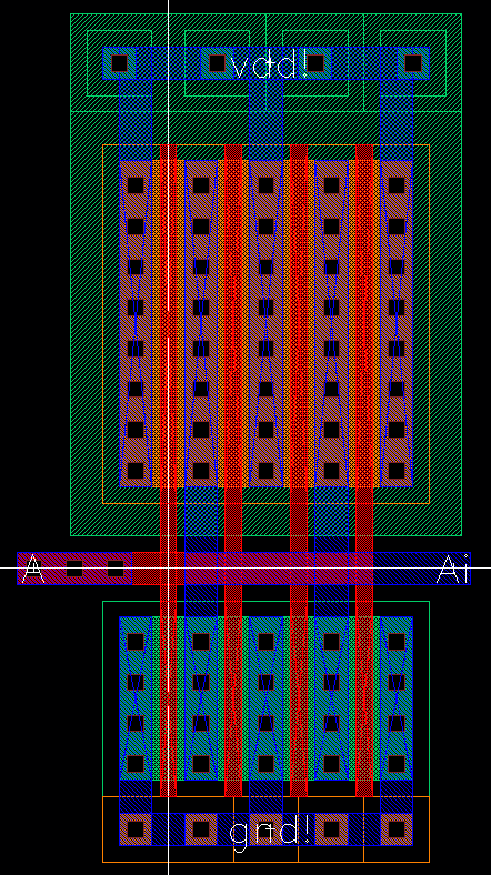
| Layout |
Extracted |

|

|
DRC successful

LVS
successful
Drafting a 2-input XOR gate using 6u/0.6u MOSFETs
Similarly, the schematic of a XOR gate was drafted using the
same methods as above.
The XOR gate consisted of 6 NMOS and PMOS's; I created a commonly used xor symbol.
| Schematic |
Symbol |

|

|
I used two
standard cell frames to layout the 2 input xor gate. I ensured that all
gate inputs, outputs, and global pins were routed on metal1.
Following the layout and extracted images are successful LVS and DRC images.
| Layout |
Extracted |

|

|
DRC
successful

LVS
successful
Drafting an inverter using 6u/0.6u MOSFETs
Similar to the previous lab, I applied the same concept to draft a 6um by 600nm inverter for simulation purposes.
| Schematic |
Symbol |

|

|
Below are layout/extracted images of the inverter.
| Layout |
Extracted |

|

|
DRC
successful

LVS
successful
GATE simulation
Using
the 3 different gates that were drafted, the logic gates were tested
using two pulse sources to imitate logical highs and lows.
A total of 4 different combinations for the 2 input gates were used to generate all possible outputs.
I simulated both the schematic and extracted layout to see if there was any differences.
| Schematic |

|
| Simulation Netlist | Simulation |
 |  |
 |  |
Truth Table| A | B | Ai | AnandB | AxorB |
| 0 | 0 | 1 | 1 | 0 |
| 0 | 1 | 1 | 1 | 1 |
| 1 | 0 | 0 | 1 | 1 |
| 1 | 1 | 0 | 1 | 1 |
I
noticed no significant differences between the two simulations;
however, there was a glitch at 200 ns due to the input signals changing
simultaneously.
The rising edge and falling edges of the input
signals results in unclear signals for 1 ns, causing the glitch in the
nand gate's output.
Drafting a full adder using 6u/0.6u MOSFETs
I used the nand gates and xor gates from the earlier portion of the lab to draft a full adder.
Likewise, I created a symbol representing an ALU which illustrates the arithematic concept of a full adder.
| Schematic |
Symbol |

|

|
Below are images of the layout and extracted views of the full adder.
I instantiated the layouts from the NAND and XOR cells to snap the different gates into place.
I also made sure the inputs and outputs of the full-adder was routed to metal1 or metal2.
DRC
successful

LVS
successful
Full-Adder simulations
Once the the Layout and Schematic matched, I proceeded to simulated the full adder.
Below are the simulation results of both the layout and the schematic.
| Schematic |

|
| Simulation Netlist | Simulation |
 |  |
 |  |
| a | b | cin | | s | cout |
| 0 | 0 | 0 | | 0 | 0 |
| 0 | 0 | 1 | | 1 | 0 |
| 0 | 1 | 0 | | 1 | 0 |
| 0 | 1 | 1 | | 0 | 1 |
| 1 | 0 | 0 | | 1 | 0 |
| 1 | 0 | 1 | | 0 | 1 |
| 1 | 1 | 0 | | 0 | 1 |
| 1 | 1 | 1 | | 1 | 1 |
Similar to the gate simulations, I didn't notice anything different between the two different simulations.
The
simulation results matched the truth table of a logical full adder;
however I noticed glitches in the same places of the gate
simulation.
When more than 1 input signal was changing simultaneously, the output signal was not clear.
Final
design directory: lab6_jb.zip
Return
to Junho's Labs
Return
to EE421L Labs


