Lab 05 - EE 421L 

Authored by Junho Bae

baej8@unlv.nevada.edu

October 11, 2017 


Pre-lab work

Back-up all my work from this lab and the course.
Complete Tutorial 3.

An inverter which was used in the lab below was drafted.

Lab Work
       
Drafting CMOS inverters
    12u/6u Inverter
   
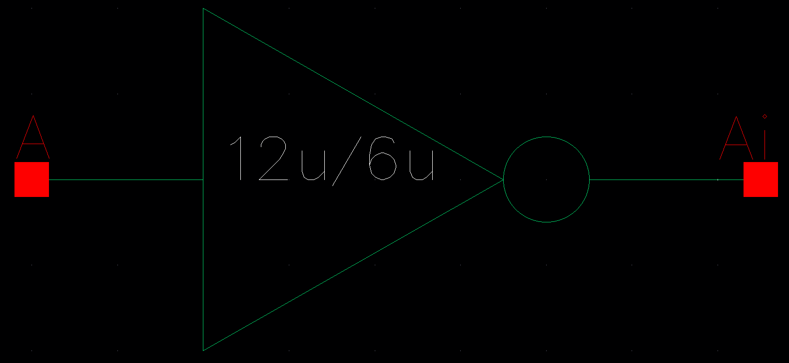
I first drafted the schematic of the inverter using a PMOS (w=12u  l=600n) and an NMOS (w=6u  l=600n).
The schematic had two pins in comparision to the layout which had four pins to cover the global power and ground. The bodies of the PMOS and NMOS were connected to their respective source terminals, their gate terminals were tied together to create an input pin, and their drain termials were connected together to create an output pin.
This process was covered in the prelab; therefore, moved on to draft the second inverter.
Schematic Symbol
http://cmosedu.com/jbaker/courses/ee421L/f17/students/baej8/Lab%205/images/lab/m1_schematic.PNG http://cmosedu.com/jbaker/courses/ee421L/f17/students/baej8/Lab%205/images/lab/m1_symbol.PNG
 
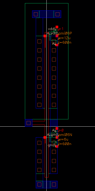
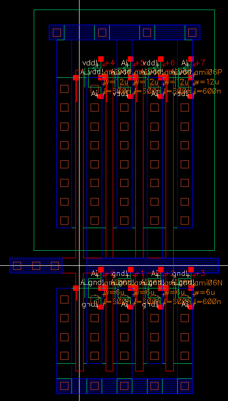
To draft the layout of the inverter, I used pre-existing cells (ntap, ptap, m1_poly, pmos, and nmos) with a few addtional connections to connect the 4 terminals to match the schematic. 
Layout Extracted
http://cmosedu.com/jbaker/courses/ee421L/f17/students/baej8/Lab%205/images/lab/m1_layout.PNG http://cmosedu.com/jbaker/courses/ee421L/f17/students/baej8/Lab%205/images/lab/m1_extracted.PNG
     
DRC successful
http://cmosedu.com/jbaker/courses/ee421L/f17/students/baej8/Lab%205/images/lab/m1_DRC.PNG
   
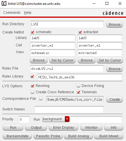
LVS successful
http://cmosedu.com/jbaker/courses/ee421L/f17/students/baej8/Lab%205/images/lab/m1_LVS_settings.PNG http://cmosedu.com/jbaker/courses/ee421L/f17/students/baej8/Lab%205/images/lab/m1_LVS_output.PNG
     
Drafting CMOS inverters
    48u/24u inverter
   
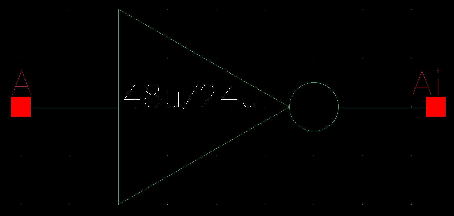
Similarly, the schematic of the second inverter was drafted using the same methods as above.
This time around, the 'multiplier' parameter of the MOSFETS were adjusted.
Schematic Symbol
http://cmosedu.com/jbaker/courses/ee421L/f17/students/baej8/Lab%205/images/lab/m4_schematic.PNG http://cmosedu.com/jbaker/courses/ee421L/f17/students/baej8/Lab%205/images/lab/m4_symbol.PNG
   
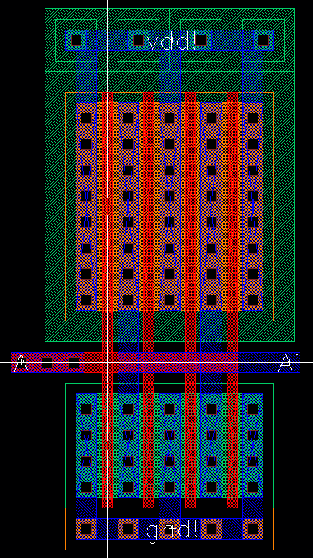
Just like the layout for the first inverter, I connected the terminals of the MOSFET accordingly.
The deciding factor of which terminals were the source and drain terminals was decided on the greater area.
Layout Extracted
http://cmosedu.com/jbaker/courses/ee421L/f17/students/baej8/Lab%205/images/lab/m4_layout.PNG http://cmosedu.com/jbaker/courses/ee421L/f17/students/baej8/Lab%205/images/lab/m4_extracted.PNG
   
DRC successful
http://cmosedu.com/jbaker/courses/ee421L/f17/students/baej8/Lab%205/images/lab/m4_DRC.PNGhttp://cmosedu.com/jbaker/courses/ee421L/f17/students/baej8/Lab%205/images/lab/m4_DRC.PNG
   
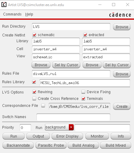
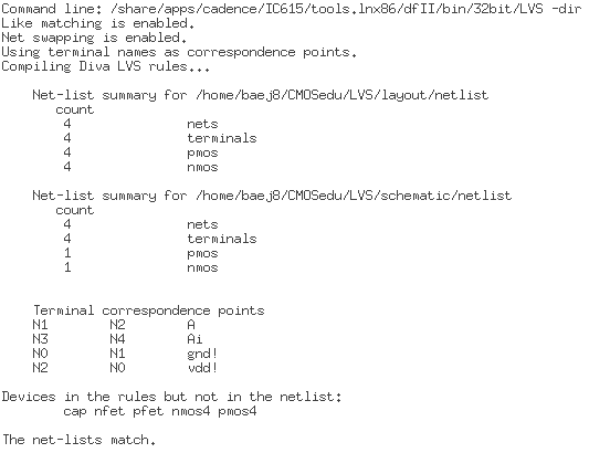
LVS successful
http://cmosedu.com/jbaker/courses/ee421L/f17/students/baej8/Lab%205/images/lab/m4_LVS_settings.PNG http://cmosedu.com/jbaker/courses/ee421L/f17/students/baej8/Lab%205/images/lab/m4_LVS_output.PNG
   
SPICE simulations
    12u/6u Inverter
   
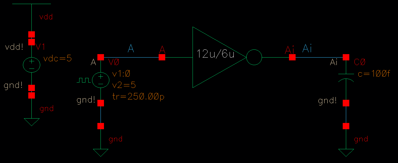
Capacitive Load Schematic Spectre UltraSim
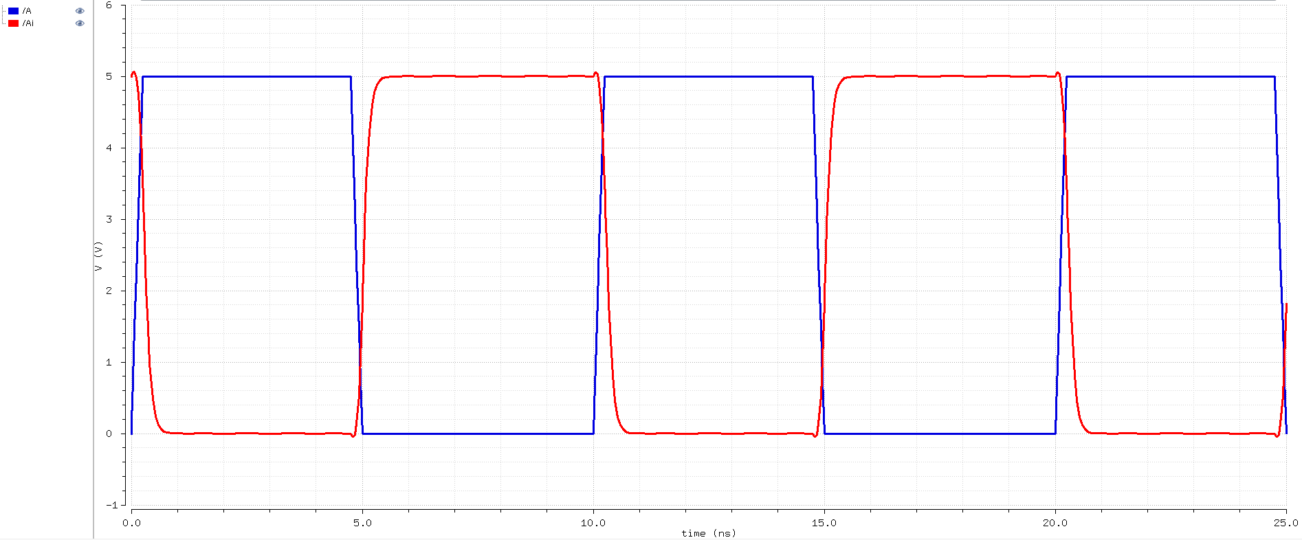
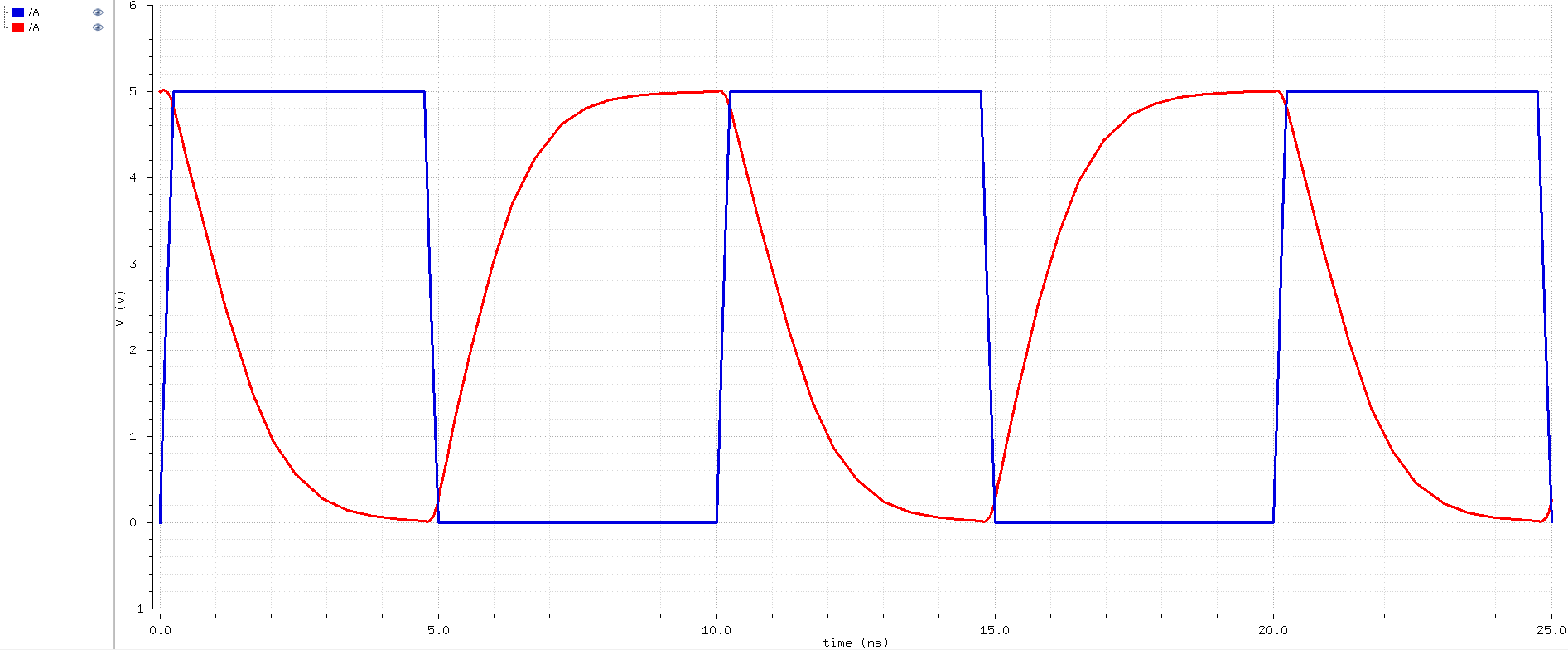
100 fF http://cmosedu.com/jbaker/courses/ee421L/f17/students/baej8/Lab%205/images/lab/sim_m1_100f_schematic.PNG http://cmosedu.com/jbaker/courses/ee421L/f17/students/baej8/Lab%205/images/lab/sim_m1_100f_normal.PNG http://cmosedu.com/jbaker/courses/ee421L/f17/students/baej8/Lab%205/images/lab/sim_m1_100f_ultra.PNG
1 pF http://cmosedu.com/jbaker/courses/ee421L/f17/students/baej8/Lab%205/images/lab/sim_m1_1p_schematic.PNG http://cmosedu.com/jbaker/courses/ee421L/f17/students/baej8/Lab%205/images/lab/sim_m1_1p_normal.PNG http://cmosedu.com/jbaker/courses/ee421L/f17/students/baej8/Lab%205/images/lab/sim_m1_1p_ultra.PNG
10 pF http://cmosedu.com/jbaker/courses/ee421L/f17/students/baej8/Lab%205/images/lab/sim_m1_10p_schematic.PNG http://cmosedu.com/jbaker/courses/ee421L/f17/students/baej8/Lab%205/images/lab/sim_m1_10p_normal.PNG http://cmosedu.com/jbaker/courses/ee421L/f17/students/baej8/Lab%205/images/lab/sim_m1_10p_ultra.PNG
100 pF http://cmosedu.com/jbaker/courses/ee421L/f17/students/baej8/Lab%205/images/lab/sim_m1_100p_schematic.PNG http://cmosedu.com/jbaker/courses/ee421L/f17/students/baej8/Lab%205/images/lab/sim_m1_100p_normal.PNG http://cmosedu.com/jbaker/courses/ee421L/f17/students/baej8/Lab%205/images/lab/sim_m1_100p_ultra.PNG
   
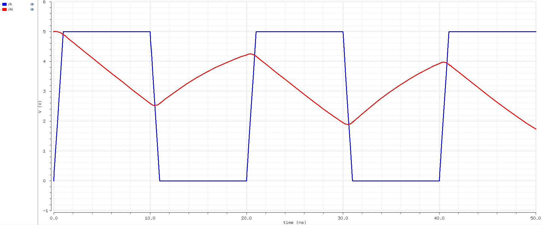
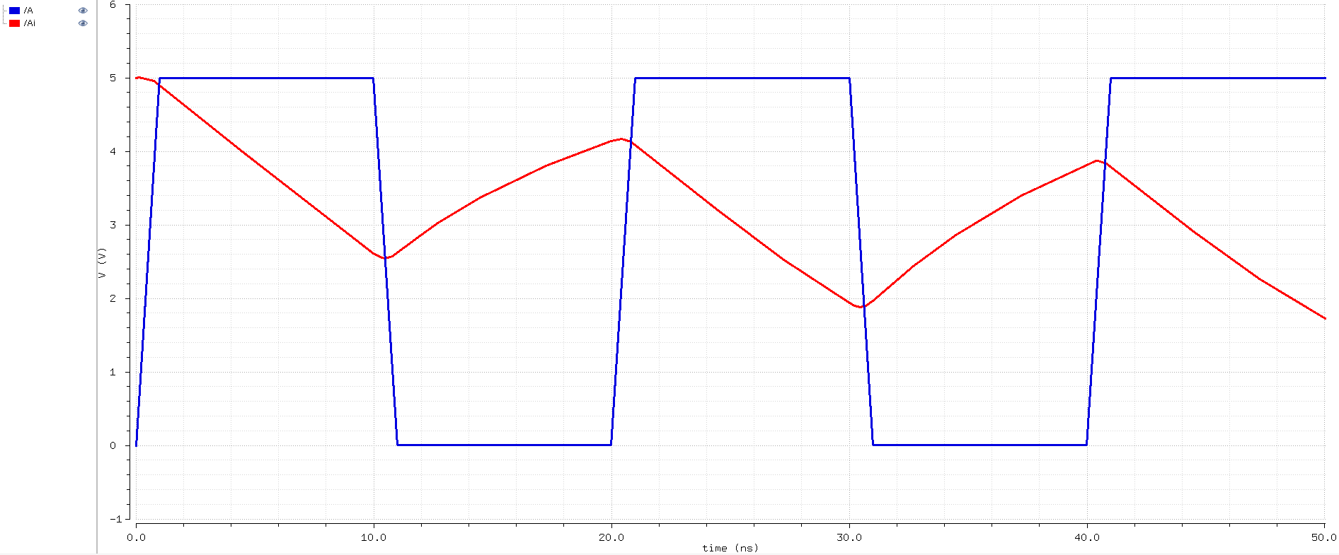
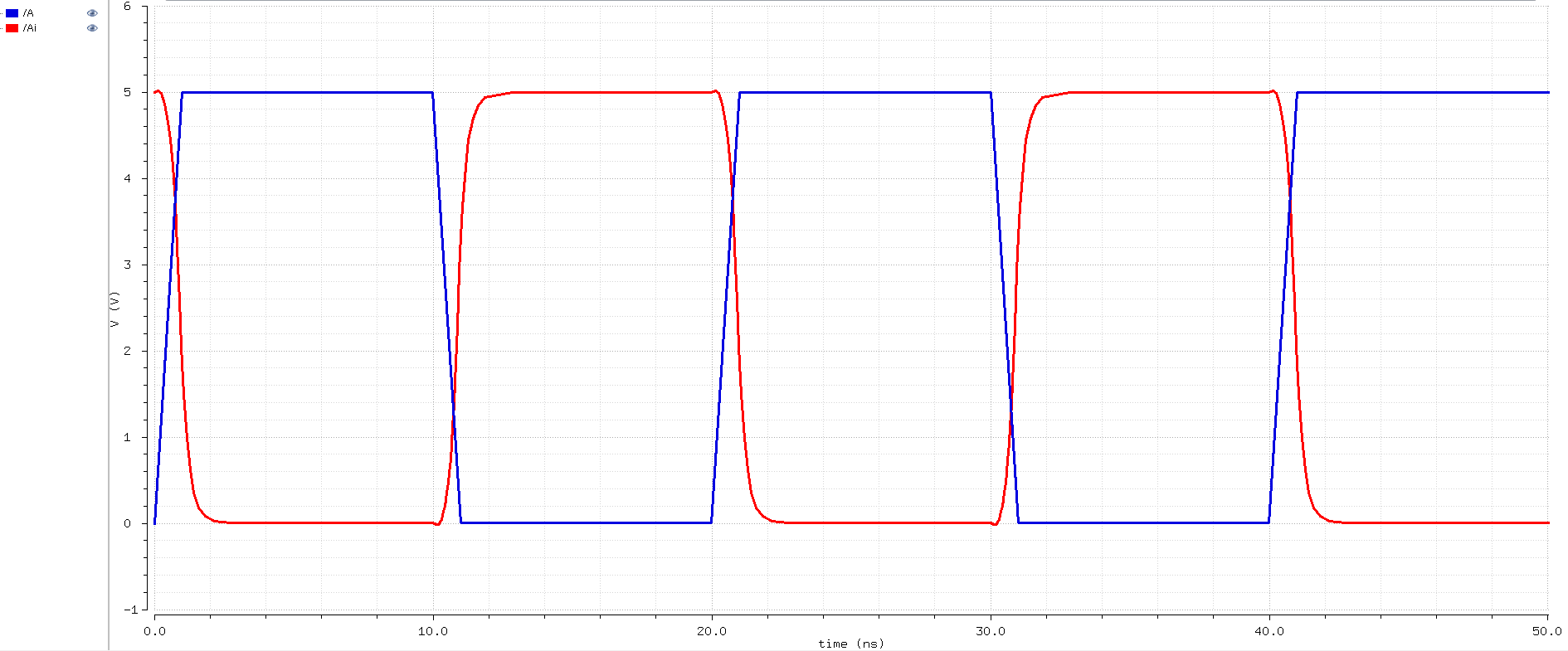
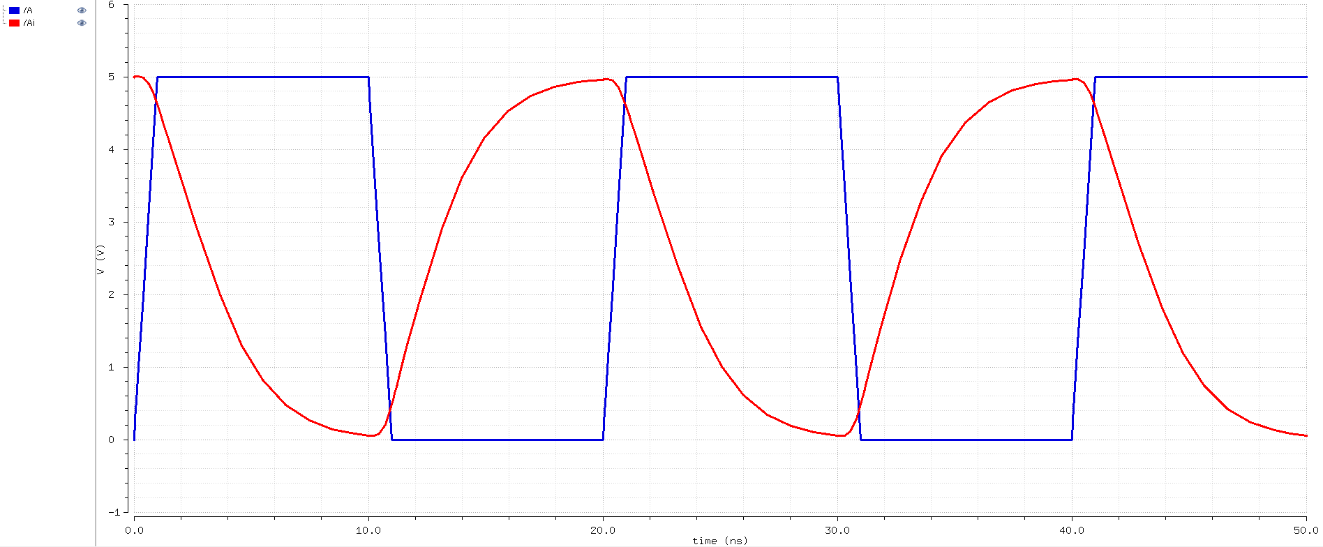
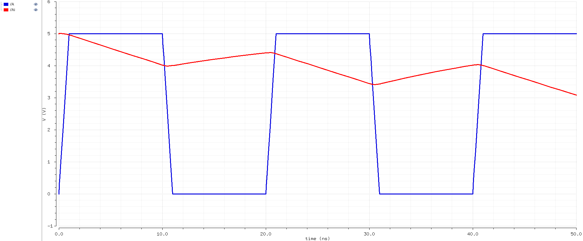
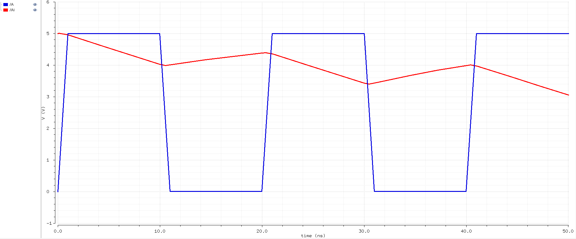
As the capacitor values increased, the inverted signal was affected more and more. Because it takes longer to charge and discharge the capacitors due to an increase in time delay, the capacitors could not be charged fast enough which resulted in poor output signals. This could be resolved by decreasing the frequency of the input signal, or keeping the capacitive load to a minimum.
In addition, there were minimum differences between the normal simulation tool that Cadence uses (Spectre) and Cadence's fast SPICE simulator (UltraSim).
     
SPICE simulations
    48u/24u inverter
   
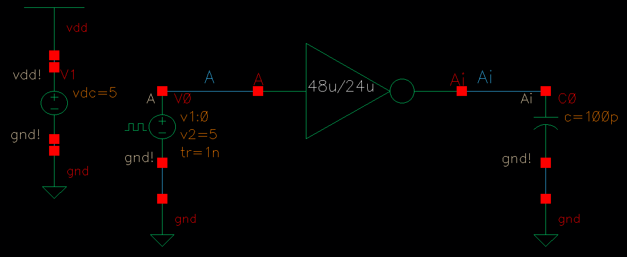
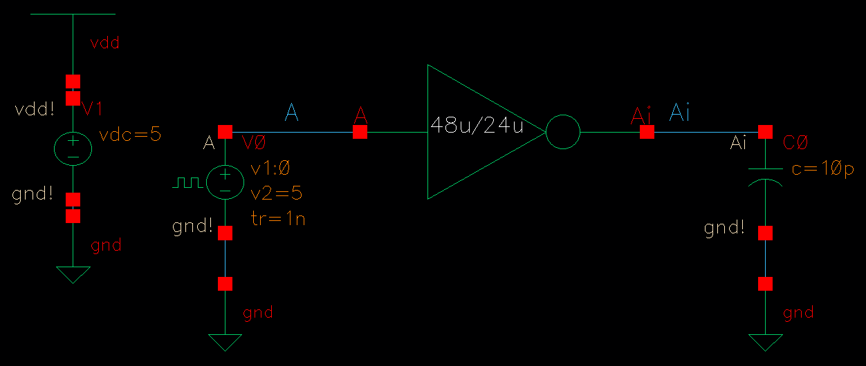
Capacitive Load Schematic Spectre UltraSim
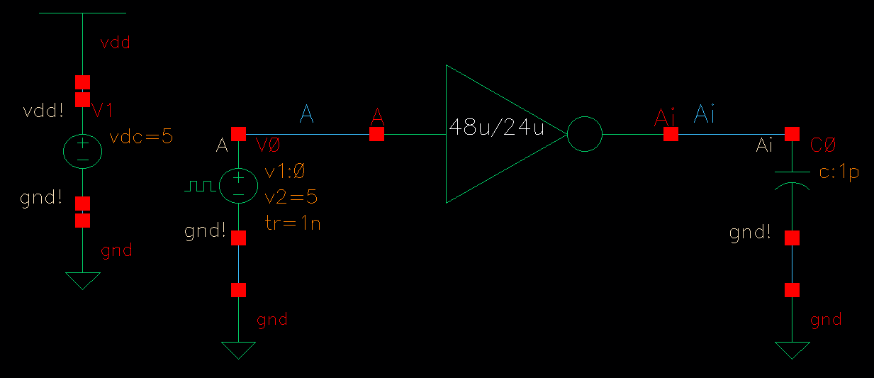
100 fF http://cmosedu.com/jbaker/courses/ee421L/f17/students/baej8/Lab%205/images/lab/sim_m4_100f_schematic.PNG http://cmosedu.com/jbaker/courses/ee421L/f17/students/baej8/Lab%205/images/lab/sim_m4_100f_normal.PNG http://cmosedu.com/jbaker/courses/ee421L/f17/students/baej8/Lab%205/images/lab/sim_m4_100f_ultra.PNG
1 pF http://cmosedu.com/jbaker/courses/ee421L/f17/students/baej8/Lab%205/images/lab/sim_m4_1p_schematic.PNG http://cmosedu.com/jbaker/courses/ee421L/f17/students/baej8/Lab%205/images/lab/sim_m4_1p_normal.PNG http://cmosedu.com/jbaker/courses/ee421L/f17/students/baej8/Lab%205/images/lab/sim_m4_1p_ultra.PNG
10 pF http://cmosedu.com/jbaker/courses/ee421L/f17/students/baej8/Lab%205/images/lab/sim_m4_10p_schematic.PNG http://cmosedu.com/jbaker/courses/ee421L/f17/students/baej8/Lab%205/images/lab/sim_m4_10p_normal.PNG http://cmosedu.com/jbaker/courses/ee421L/f17/students/baej8/Lab%205/images/lab/sim_m4_10p_ultra.PNG
100 pF http://cmosedu.com/jbaker/courses/ee421L/f17/students/baej8/Lab%205/images/lab/sim_m4_100p_schematic.PNG http://cmosedu.com/jbaker/courses/ee421L/f17/students/baej8/Lab%205/images/lab/sim_m4_100p_normal.PNG http://cmosedu.com/jbaker/courses/ee421L/f17/students/baej8/Lab%205/images/lab/sim_m4_100p_ultra.PNG
   
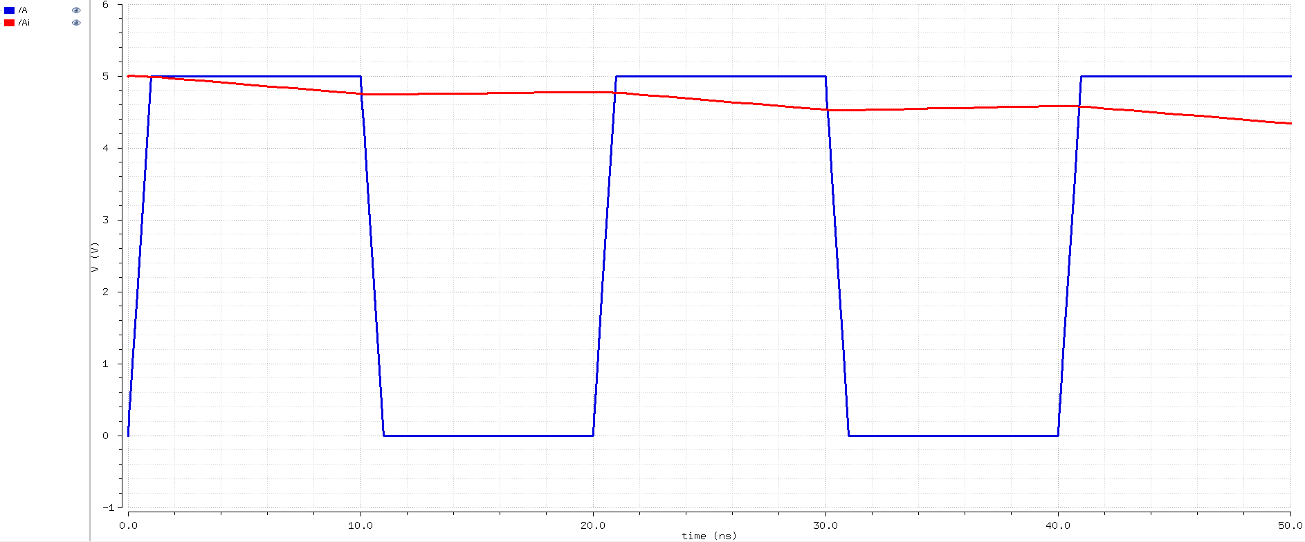
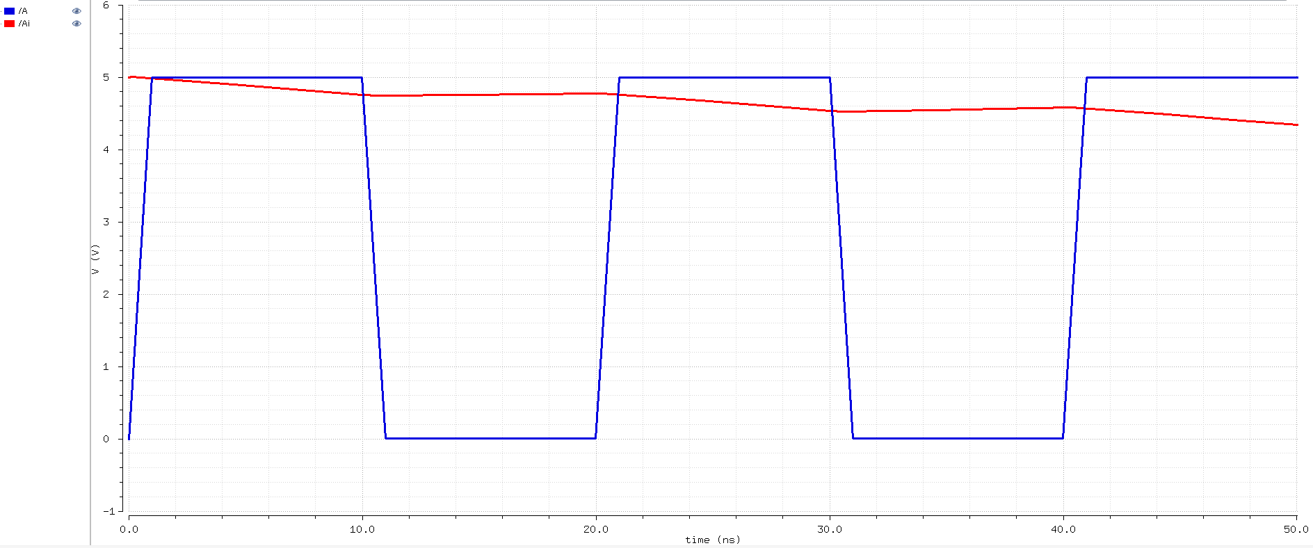
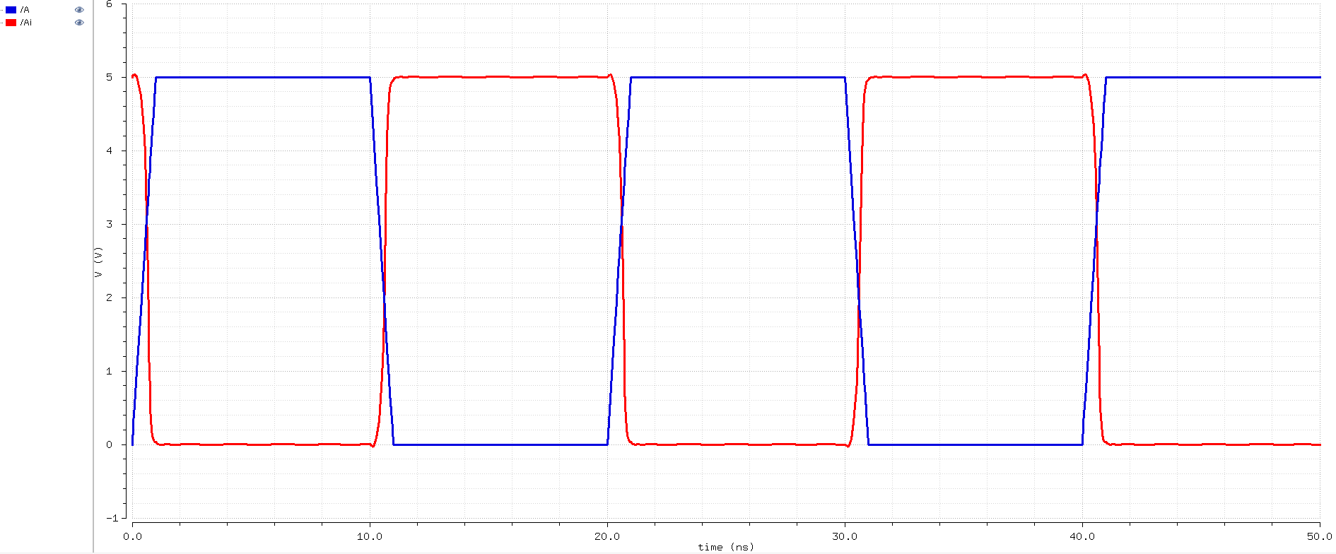
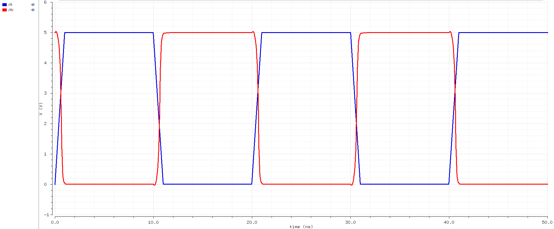
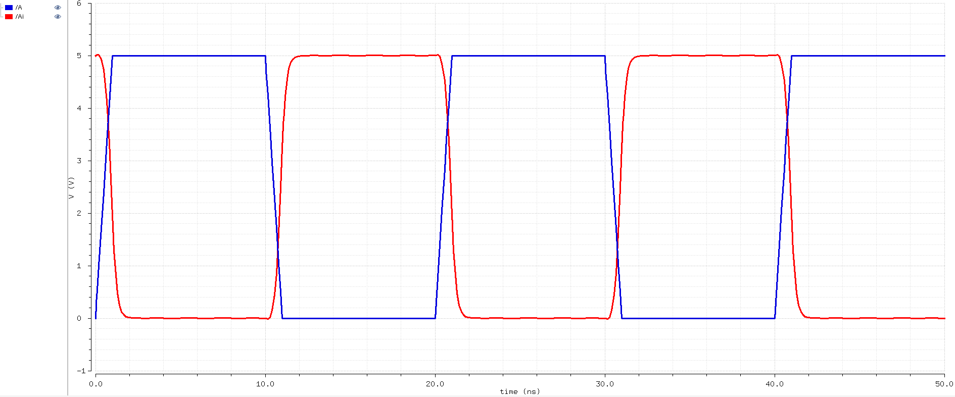
The pattern from the first inverter still persisted; however, the inverter was able to handle greater capacitive loads due to more current flowing through the inverter. The time delay of the simulations were shorter than the inverter with a 'multiplier' parameter of 1, but became irrelevant as the capacitive load increased past a certain extent.
Although the simulations were faster, there wasn't much of a loss in accuracy when using the UltraSim tool.
   
Final design directory: lab5_jb.zip
     

Return to Junho's Labs
Return to EE421L Labs