Lab 04 - EE 421L 

Authored by Junho Bae

baej8@unlv.nevada.edu

September 27, 2017 


Pre-lab work

Back-up all my work from this lab and the course.
Complete Tutorial 2.
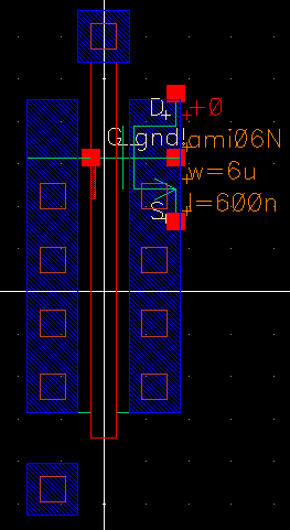
Below are images of the MOSFET making process from Tutorial 2.
   
NMOS
Schematic Symbol Layout Extracted
http://cmosedu.com/jbaker/courses/ee421L/f17/students/baej8/Lab%204/images/prelab/nmos_schematic.PNG http://cmosedu.com/jbaker/courses/ee421L/f17/students/baej8/Lab%204/images/prelab/nmos_symbol.PNG http://cmosedu.com/jbaker/courses/ee421L/f17/students/baej8/Lab%204/images/prelab/nmos_layout.PNG http://cmosedu.com/jbaker/courses/ee421L/f17/students/baej8/Lab%204/images/prelab/nmos_extracted.PNG
   
PMOS
Schematic Symbol Layout Extracted
http://cmosedu.com/jbaker/courses/ee421L/f17/students/baej8/Lab%204/images/prelab/pmos_schematic.PNG http://cmosedu.com/jbaker/courses/ee421L/f17/students/baej8/Lab%204/images/prelab/pmos_symbol.PNG http://cmosedu.com/jbaker/courses/ee421L/f17/students/baej8/Lab%204/images/prelab/pmos_layout.PNG http://cmosedu.com/jbaker/courses/ee421L/f17/students/baej8/Lab%204/images/prelab/pmos_extracted.PNG


Lab Work
   
Generating 4 schematics and simulations
    NMOS (
6u/600n width-to-length ratio)
   
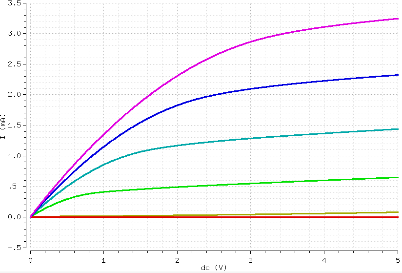
1. ID v. VDS of an NMOS device for VGS varying from 0 to 5 V in 1 V steps while VDS varies from 0 to 5 V in 1 mV steps.
 
In order to generate an IV plot, the body of the NMOS was tied to ground, and two different voltage sources were swept.

Below on the left is the schematic used from the symbol I created from the prelab to generate the IV plot (right).
http://cmosedu.com/jbaker/courses/ee421L/f17/students/baej8/Lab%204/images/lab/sim1_schematic.PNG http://cmosedu.com/jbaker/courses/ee421L/f17/students/baej8/Lab%204/images/lab/sim1.PNG
     
Below are the settings from ADE L used to plot the 3 different variables. Along with a dc sweep, a parametric analysis was used to vary VGS.
http://cmosedu.com/jbaker/courses/ee421L/f17/students/baej8/Lab%204/images/lab/sim1_ade.PNG
http://cmosedu.com/jbaker/courses/ee421L/f17/students/baej8/Lab%204/images/lab/sim1_para.PNG
 
2.
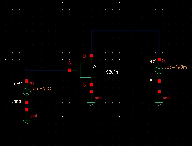
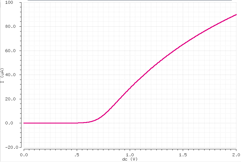
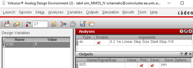
ID v. VGS of an NMOS device for VDS = 100 mV where VGS varies from 0 to 2 V in 1 mV steps.
   
For this simulation I held VDS at a constant voltage while sweeping VGS to plot current flowing throught the NMOS.
Below on the left is the schematic used to plot the ID v. VGS plot (right). The NMOS was taken from the symbol view of the prelab.

http://cmosedu.com/jbaker/courses/ee421L/f17/students/baej8/Lab%204/images/lab/sim2_schematic.PNG http://cmosedu.com/jbaker/courses/ee421L/f17/students/baej8/Lab%204/images/lab/sim2.PNG
   
Below are the settings of the Analog Design Environment used to sweep VGS.
http://cmosedu.com/jbaker/courses/ee421L/f17/students/baej8/Lab%204/images/lab/sim2_ade.PNG
     
Generating 4 schematics and simulations
    PMOS (12u/600n width-to-length ratio)
     
3.
ID v. VSD (note VSD not VDS) of a PMOS device for VSG (not VGS) varying from 0 to 5 V in 1 V steps while VSD varies from 0 to 5 V in 1 mV steps.
   
In order to generate an IV plot, the body of the PMOS was tied to Vdd, and two different voltage sources were swept.
Below on the left is the schematic used from the symbol I created from the prelab to generate the IV plot (right).
http://cmosedu.com/jbaker/courses/ee421L/f17/students/baej8/Lab%204/images/lab/sim3_schematic.PNG http://cmosedu.com/jbaker/courses/ee421L/f17/students/baej8/Lab%204/images/lab/sim3.PNG
     
Below are the settings from ADE L used to plot the 3 different variables. Along with a dc sweep, the parametric analysis was used to vary VSG.
http://cmosedu.com/jbaker/courses/ee421L/f17/students/baej8/Lab%204/images/lab/sim3_ade.PNG
http://cmosedu.com/jbaker/courses/ee421L/f17/students/baej8/Lab%204/images/lab/sim3_para.PNG
   
4.
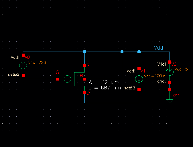
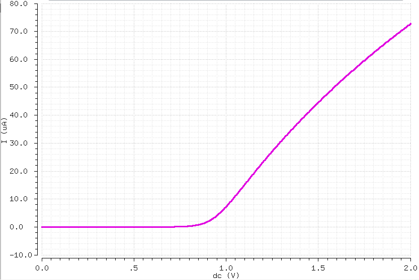
ID v. VSG of a PMOS device for VSD = 100 mV where VSG varies from 0 to 2 V in 1 mV steps.
   
For this simulation I held VSD at a constant voltage while sweeping VSG to plot current flowing throught the PMOS.
Below on the left is the schematic used to plot the ID v. VSG plot (right). The PMOS was taken from the symbol view of the prelab.

http://cmosedu.com/jbaker/courses/ee421L/f17/students/baej8/Lab%204/images/lab/sim4_schematic.PNG http://cmosedu.com/jbaker/courses/ee421L/f17/students/baej8/Lab%204/images/lab/sim4.PNG
     
Below are the settings of the Analog Design Environment used to sweep VSG.
http://cmosedu.com/jbaker/courses/ee421L/f17/students/baej8/Lab%204/images/lab/sim4_ade.PNG
   
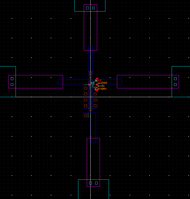
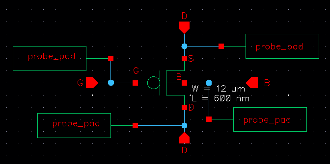
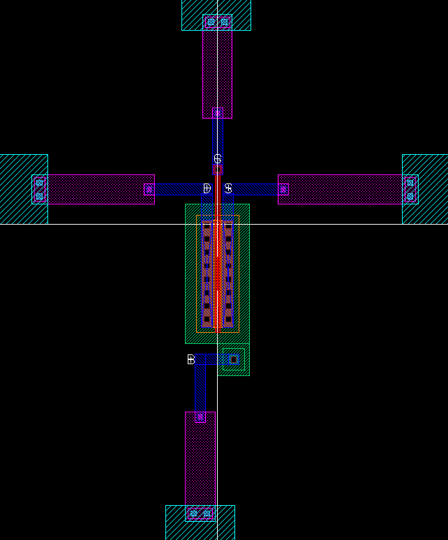
NMOS layout with probe pads
I added an addtional pin for the body of the NMOS from the prelab instead of tying the body directly to ground, to create a 4 terminal MOSFET.
To connect the probe pads to the terminals of the NMOS, all 3 metals and both Via and Via2 had to be used.
Using pre-exisitng cells, 'm2_m1' and 'm3_m2', the connections to each layer was made to ultimately reach the probe pads (metal3).
   
Schematic Layout focusing on NMOS Full Layout view
http://cmosedu.com/jbaker/courses/ee421L/f17/students/baej8/Lab%204/images/lab/nmos_schematic.PNG http://cmosedu.com/jbaker/courses/ee421L/f17/students/baej8/Lab%204/images/lab/nmos_layout_closeup.PNGhttp://cmosedu.com/jbaker/courses/ee421L/f17/students/baej8/Lab%204/images/lab/nmos_layout_closeup.PNG http://cmosedu.com/jbaker/courses/ee421L/f17/students/baej8/Lab%204/images/lab/nmos_full_layout.PNG
   
Layout passing DRC
http://cmosedu.com/jbaker/courses/ee421L/f17/students/baej8/Lab%204/images/lab/nmos_DRC.PNG
     
Extracted view focusing on NMOS Full Extracted view
http://cmosedu.com/jbaker/courses/ee421L/f17/students/baej8/Lab%204/images/lab/nmos_extracted_closeup.PNG http://cmosedu.com/jbaker/courses/ee421L/f17/students/baej8/Lab%204/images/lab/nmos_extracted.PNG
     
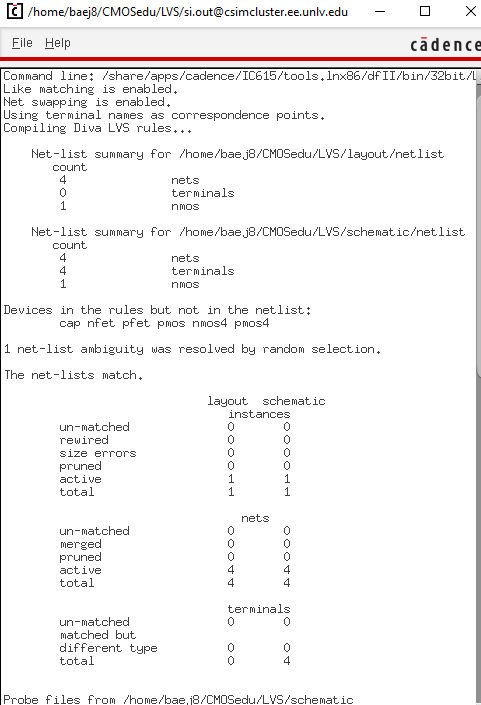
Successful LVS
http://cmosedu.com/jbaker/courses/ee421L/f17/students/baej8/Lab%204/images/lab/nmos_LVS.PNG http://cmosedu.com/jbaker/courses/ee421L/f17/students/baej8/Lab%204/images/lab/nmos_LVS_output.PNG
   
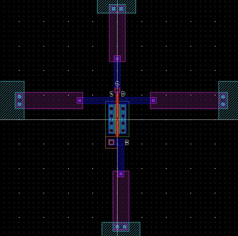
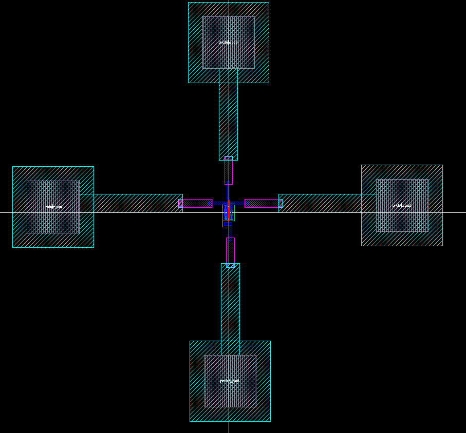
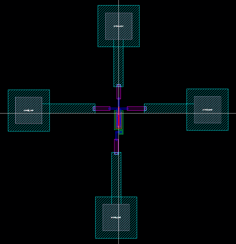
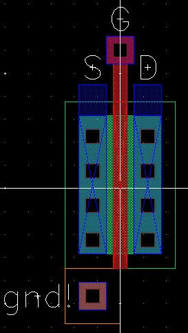
PMOS layout with probe pads
Similar to the NMOS, I used the PMOS layout that I made in prelab to attach the probe pads.
I used the pre-existing cells to connect each layer all the way up to metal 3.
     
Schematic Layout focusing on PMOS Full Layout view
http://cmosedu.com/jbaker/courses/ee421L/f17/students/baej8/Lab%204/images/lab/pmos_schematic.PNG http://cmosedu.com/jbaker/courses/ee421L/f17/students/baej8/Lab%204/images/lab/pmos_layout_closeup.PNG http://cmosedu.com/jbaker/courses/ee421L/f17/students/baej8/Lab%204/images/lab/pmos_full_layout.PNGhttp://cmosedu.com/jbaker/courses/ee421L/f17/students/baej8/Lab%204/images/lab/pmos_full_layout.PNG
     
Layout passing DRC
http://cmosedu.com/jbaker/courses/ee421L/f17/students/baej8/Lab%204/images/lab/pmos_DRC.PNG
       
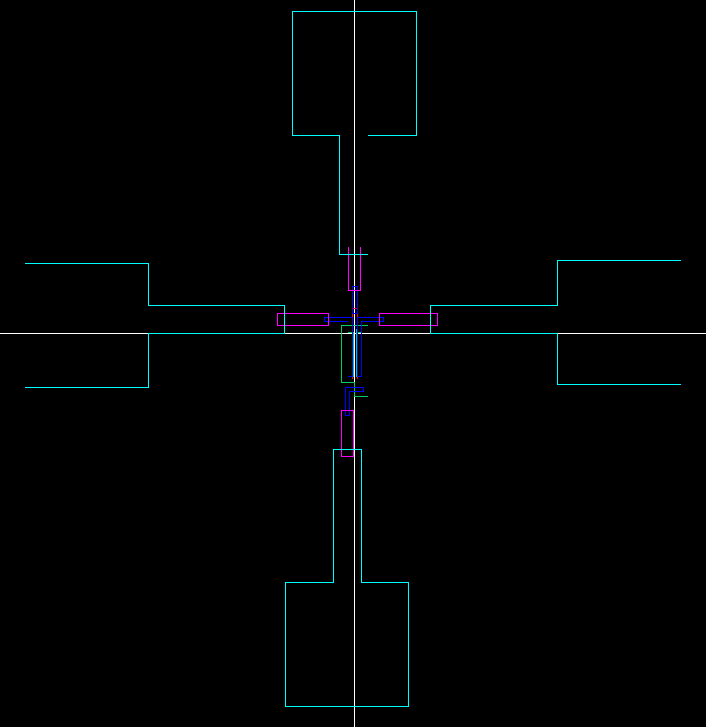
Extracted view focusing on PMOS Full Extracted view
http://cmosedu.com/jbaker/courses/ee421L/f17/students/baej8/Lab%204/images/lab/pmos_extracted_closeup.PNG http://cmosedu.com/jbaker/courses/ee421L/f17/students/baej8/Lab%204/images/lab/pmos_extracted.PNG
       
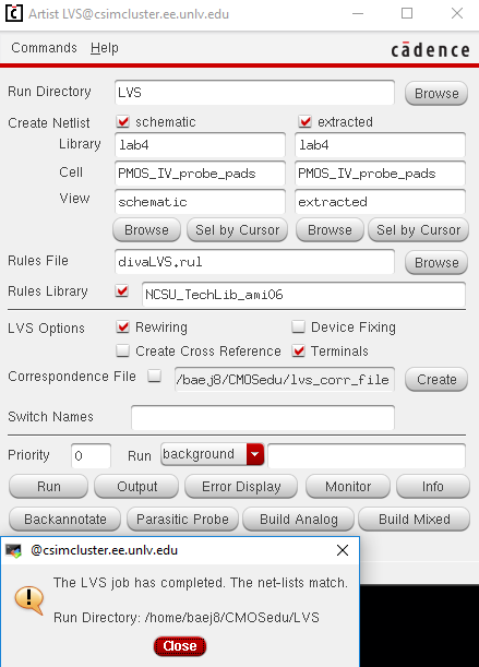
Successful LVS
http://cmosedu.com/jbaker/courses/ee421L/f17/students/baej8/Lab%204/images/lab/pmos_LVS.PNG http://cmosedu.com/jbaker/courses/ee421L/f17/students/baej8/Lab%204/images/lab/pmos_LVS_output.PNG
       
Final design directory: lab4_jb.zip
     

Return to Junho's Labs

Return to EE421L Labs