Lab 03 -
EE 421L
Authored
by Junho Bae
baej8@unlv.nevada.edu
September
20, 2017
Pre-lab
work
Back-up all of my
previous work from the lab and the course.
Complete Tutorial 1.
Lab
Work
I
created a layout of the 10-bit DAC that I designed in Lab 2, and
simulated the layout design. I then compared the simulations of both
the layout and schematic (lab2) designs.
Designing a
layout of a 10k resistor
In
order to produce the layout of the 10-bit DAC that I desgined and
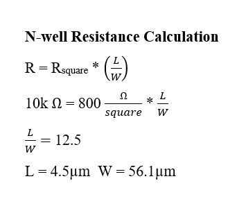
simulated in Lab 2, I calculated the length and width of the n-well to
produce the desired resistor value.
Using 800ohms/square as the
sheet resistance of the n-well from the process information given by
MOSIS, I decided on the width of 4.5 microns similar to the tutorial.
In efforts to match the size-2 n-tap, I chose a length that was 12.5
times greater than 4.5 microns. The length of the n-well was slightly
adjusted to fit cadance's design scale (56.25->56.1). The
minimum
width (12-lambda) and the minimum width (18-lambda) was accounted for.
The image below shows the dimensions and calculations of the
resistor layout.
Layout of full 10k resistor after adding res_id layer, n-taps, and pins
onto the metal 1 layer.

Extracted view of the 10k resistor

Designing the layout of
my DAC
I
used the layout created above to first create a voltage divider of two
10k resistors in series and one 10k resistor in parllel. This voltage
divider layout was copied 9 more times and placed right under each
other. I turned off horizontal movements, and locked the vertical
movements to orthogonal so that each resistor in the DAC was laid out
in parallel having the same x-position but varying y-positions. The
metal 1 layer was used to connect each section of the DAC together to
match the design of lab 2. After adding one final resistor onto the
last voltage divider, pins were added onto the metal 1 layer
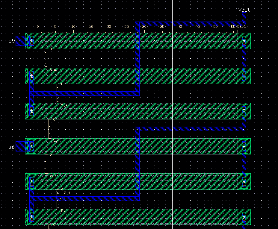
corresponding to their inputs and output. To ensure the n-wells were
not too close to each other, the ruler feature (k) was used to measure
a minimum distance of 5.4 microns from each resistor.
Layout of 10-bit DAC

After
comopleting the full layout of the DAC, I DRC'ed the layout to make
sure that the layout of free of errors.

Extracted view of the
DAC layout

Complete view of
the layout on the left and complete extracted view on the right
To
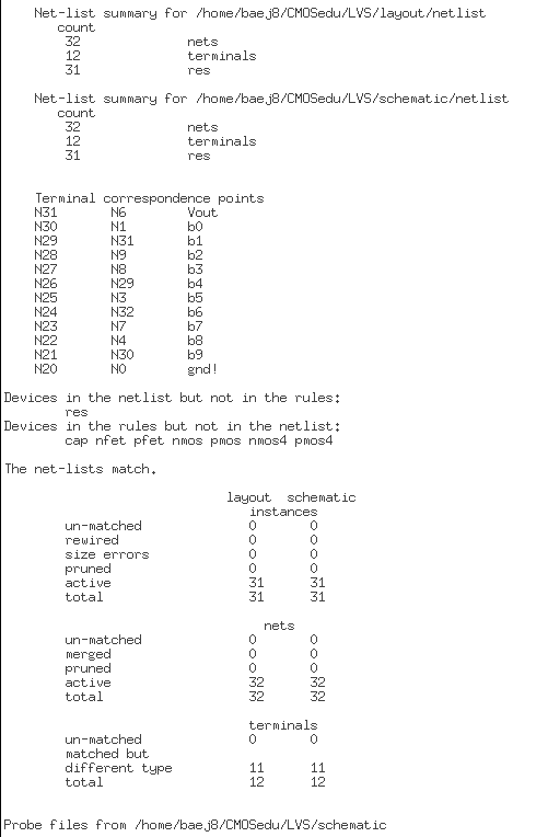
make sure the layout matched the orginal design in lab 2, I used the
layout-versus-schematic feature to verify both designs. Using the
layout in this lab and the schematic design from lab 2, the output on
the right (LVS output) illustrated both netlists matching.
Simulations of
the Layout
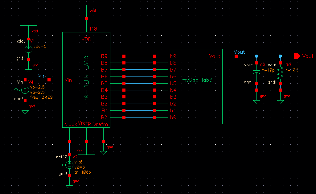
Using
the ideal_ADC_DAC schematic with the DAC replaced by the symbol that I
created in lab 2, I simulated the layout to see if the output signal
was close to the schematic design.
Below is the image of the original schematic with the DAC replaced.

I copied all of the necessary files into a new sim_cell where I wanted
to simulated the layout design. By heading into ADE L -> Setup ->
Environment Options,
I added the key words "exracted", as seen in the image on the left, to
simulated the layout in place of the orignal schematic. The
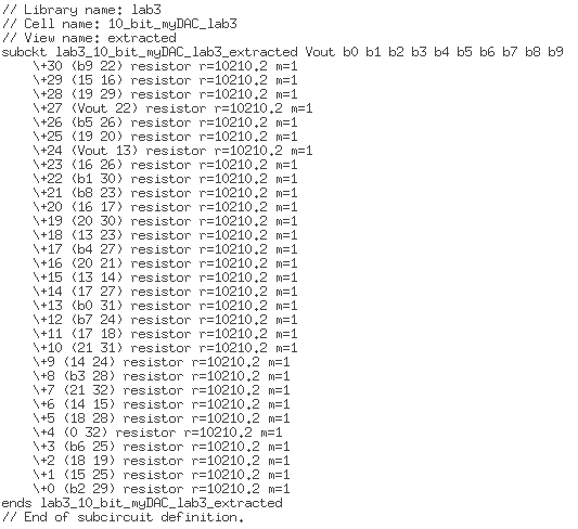
simulation netlist outout on the right shows that the extracted view of
the layout was used for the DAC component.
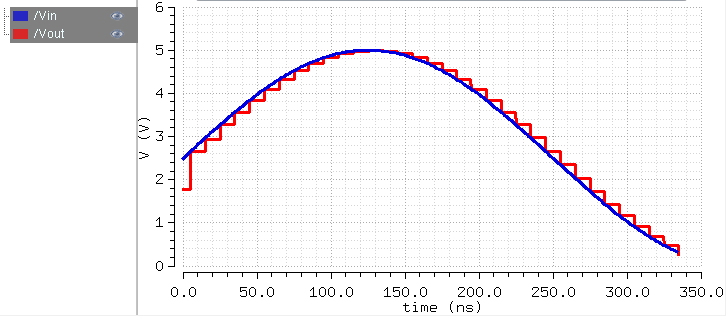
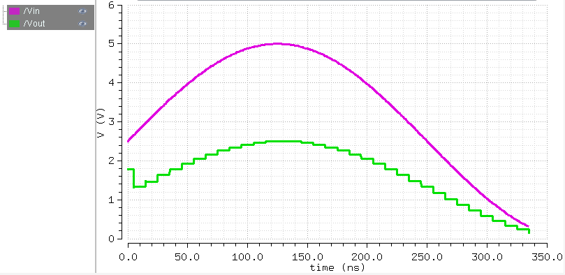
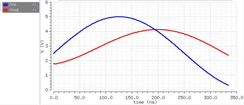
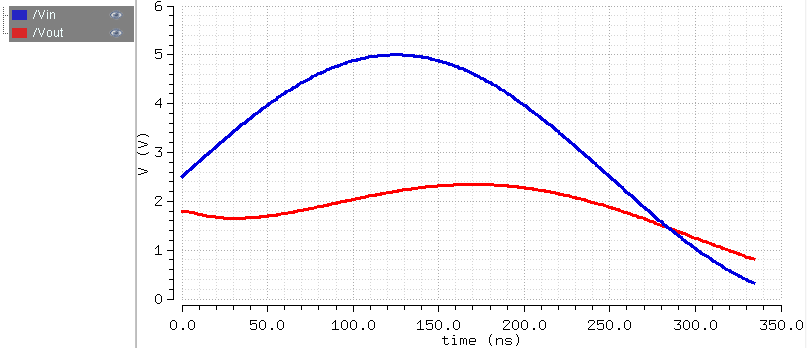
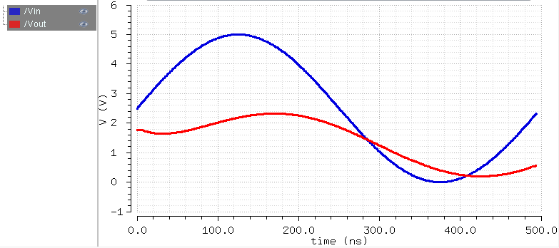
The simulations below show almost exact results from both the schematic
and the layout design.
Each simulation is not described in detail because they are explained
in Lab 2.
Left: Schematic
Right:
Layout
Driving no load
Driving a resisitive load
Driving a capacitive load
Driving a RC load
Final
design directory: lab3_jb.zip
Return
to Junho's Labs
Return
to EE421L Labs
