Lab Project - EE 421L
Authored
by Sharyn Miyaji,
Email: miyajis@unlv.nevada.edu
Schematic: Wednesday, November 16, 2016
Layout: Wednesday, November 30, 2016
Project Description
For
our project, our goal is to be a able to design a detector that is able
to take a serial input and detect the sequence 101011. When the
detector reads the sequence, the output of the detector will output a
high logic signal. This project is made up of 3 components, which
are D flip flops, a NAND gate, and an inverter.
Part 1: Schematic
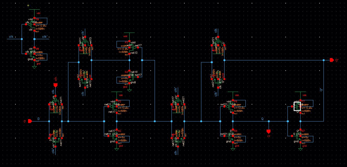
Creating a D Flip Flop
First, a schematic of a D flip flop is laid as shown below and is then created into a symbol.
Schematic
Symbol
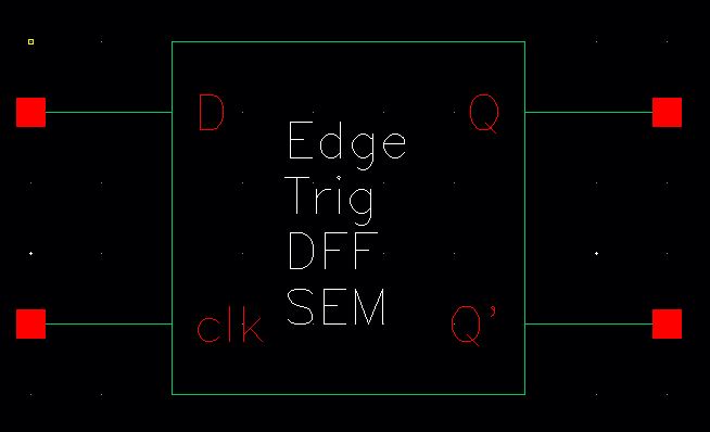
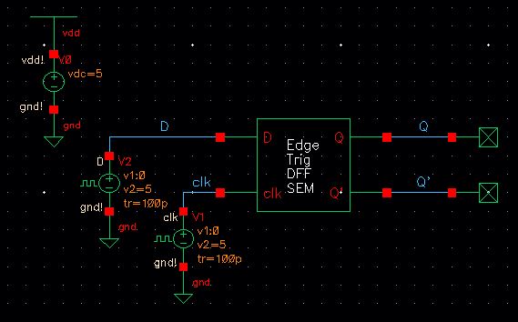
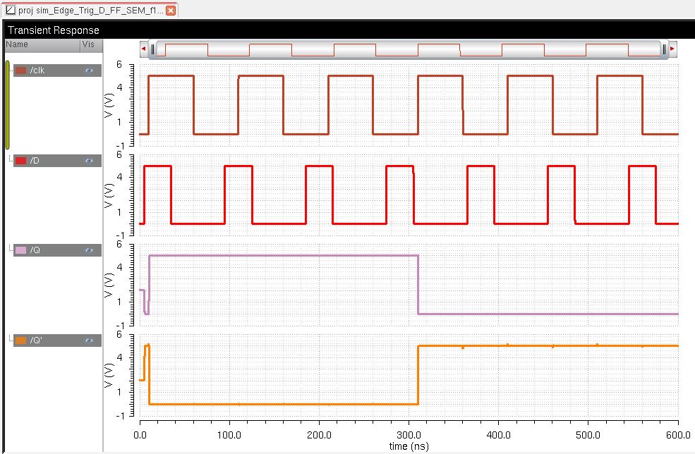
Once the symbol is created, we test out the D flip flop to see if it is working properly.
Simulation Schematic
Simulation
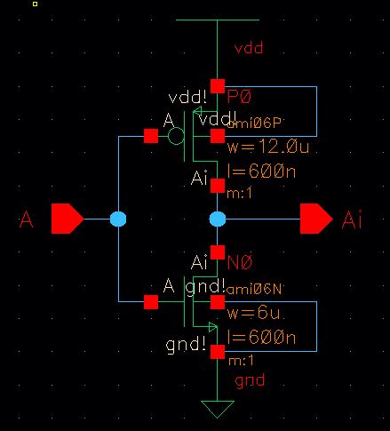
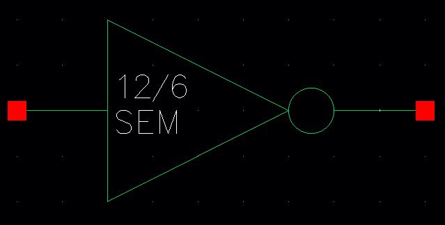
Creating an Inverter
Next an inverter is created, so the detector triggers a high output when the sequence 101011 is detected.
Schematic
Symbol
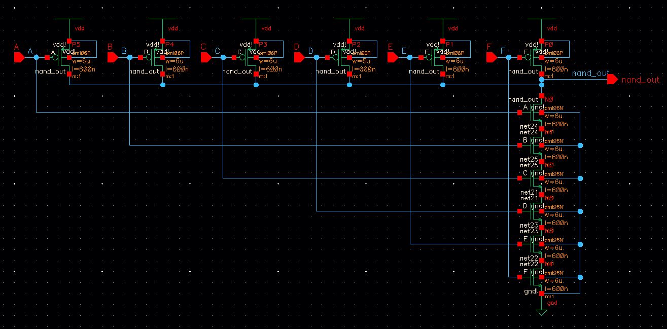
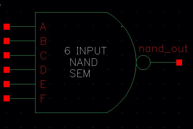
Creating a 6-Input NAND
Lastly, a 6-input NAND gate is created, so the bits from each D flip flop create a sequence that can be read.
Schematic
Symbol
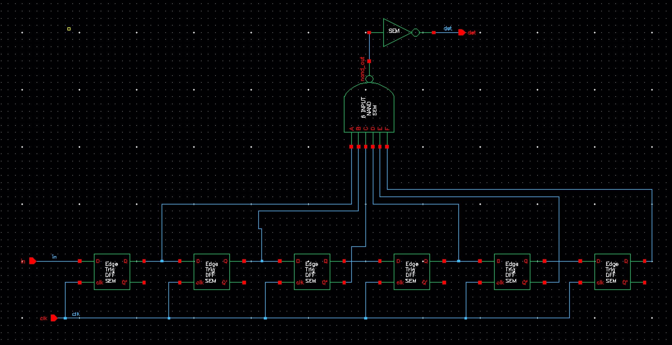
Creating the Detector
Once
all of the components for the detector are checked and saved, the
schematic of the detector is laid out as shown below. Pin A of
the NAND gate is connected to Q of the first D flip flop, pin B is
connected to Q', pin C is connected to Q, pin D is connected to Q', pin
E is connected to Q, and pin F is connected to Q, so the detector only
reads a sequence of 101011. The
inverter is then connected to the output of the 6-input NAND gate, so
that it is triggered when the detector detects the sequence. Once
everything is connected, a symbol is created to be used for simulation.
Schematic
Symbol

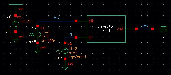
Testing the Detector
Using the detector symbol created previously, a pulse voltage source is attached to the clk input and a piece-wise linear voltage source is attached to the in input, so we can create our own sequence to test out our detector.
Schematic
Simulation
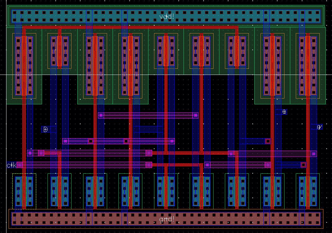
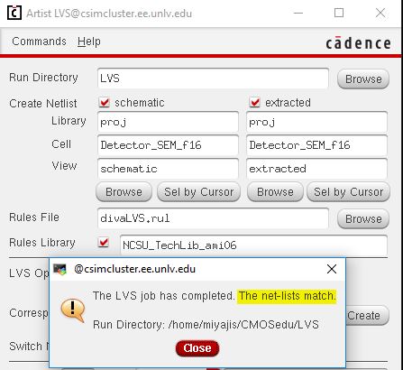
Part 2: Layouts
Second
part of the project is creating layouts of the parts of the detector.
Each part must be DRCed and LVSed before connecting it all
together.
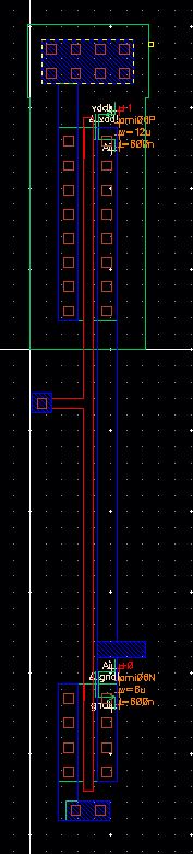
D Flip Flop
Layout
Extracted
DRC

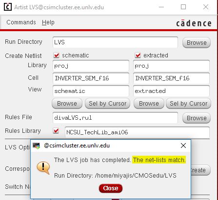
LVS
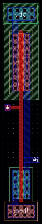
Inverter
Layout
Extracted
DRC

LVS
6 Input NAND Gate
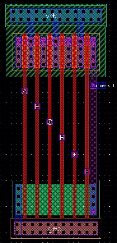
Layout
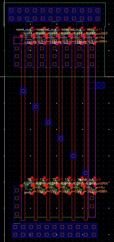
Extracted
DRC

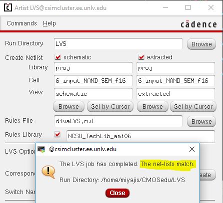
LVS
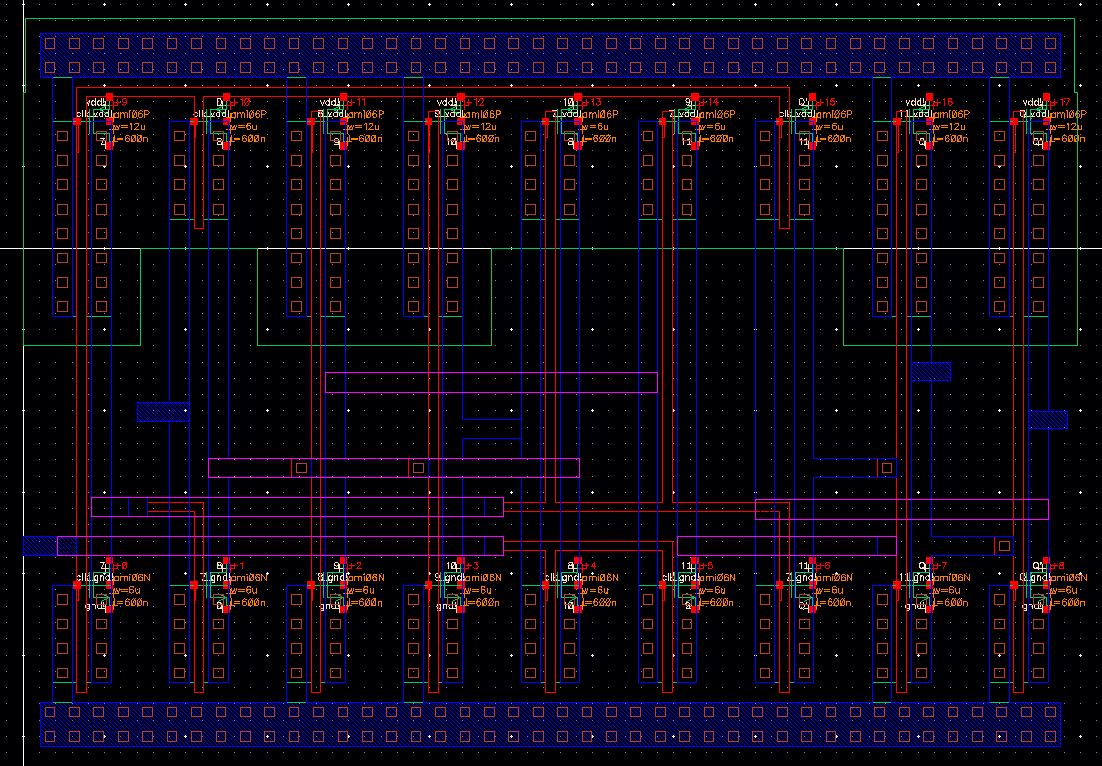
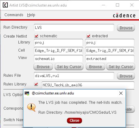
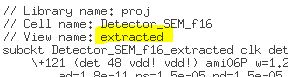
Detector
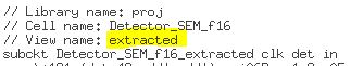
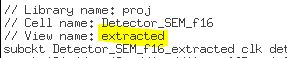
Layout
Extracted
DRC

LVS
Buffer
A
buffer is created to "clean up" the simulation for the detector;
therefore, it will not be a part of the detector schematic, but will be
additionally placed into the chip layout.
Schematic
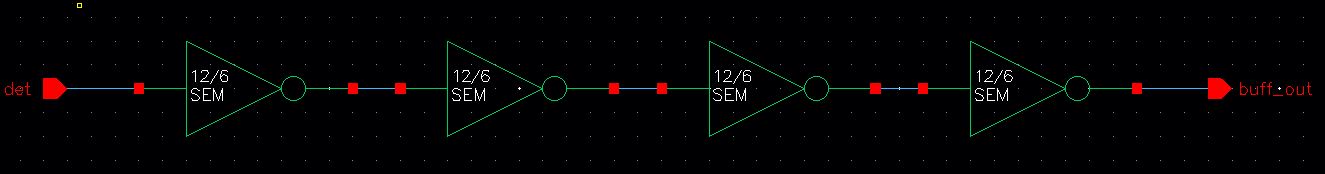
Symbol

Layout
Extracted
DRC

Layout
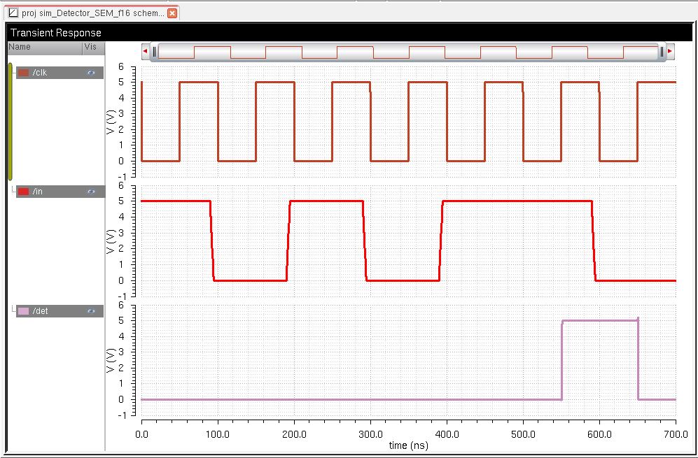
Simulations
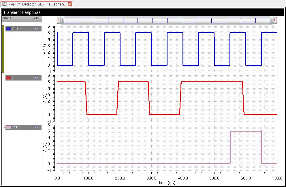
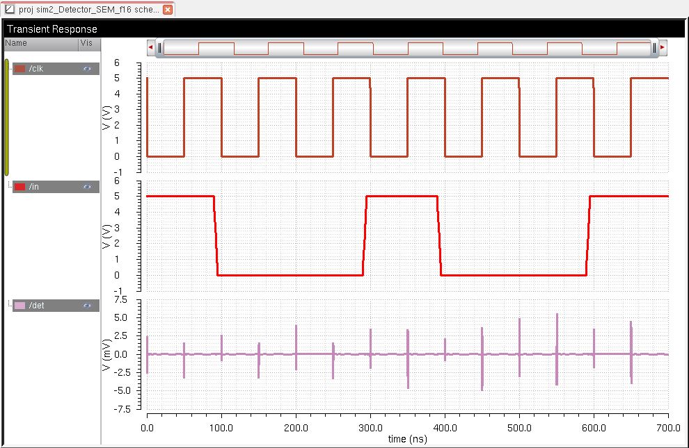
The first simulation below shows that the detector works when the sequence 101011 is detected using the extracted layout.
The next simulation is a test to see if whether or not the detector will detect a sequence that is not 101011.
As
a result, the detector passes the test of not detecting a sequence that
is not 101011. There are a few spikes in the simulation due to
possible noise going into it.
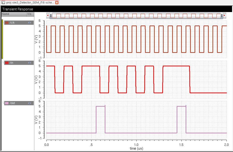
Lastly,
the simulation below is a test to see if the detector will detect the
sequence 101011 twice with random sequences in between.
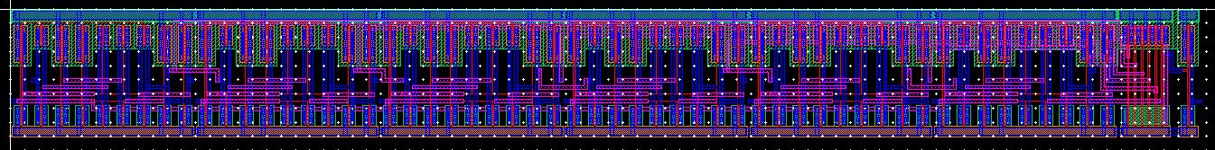
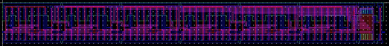
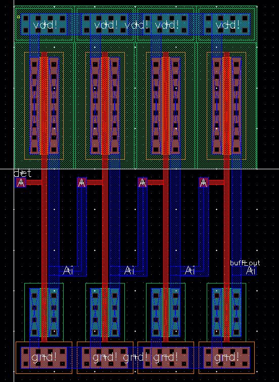
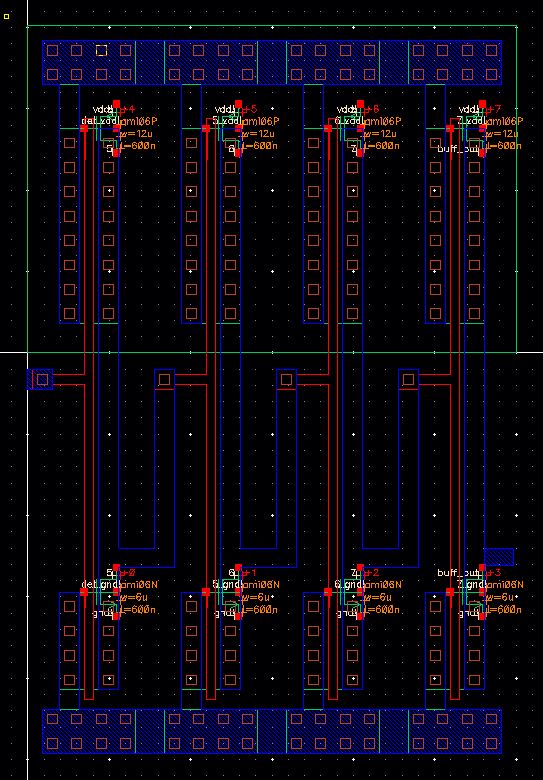
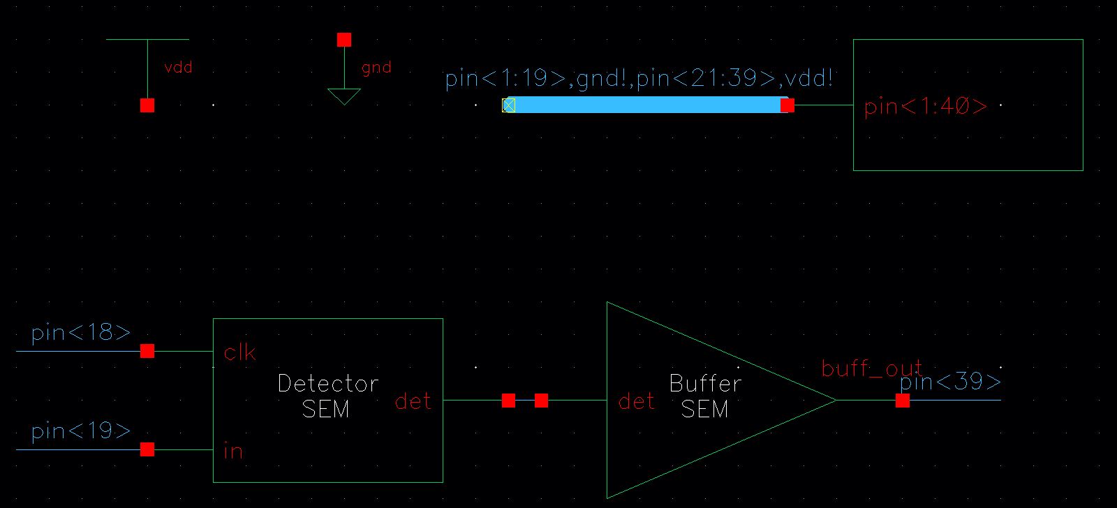
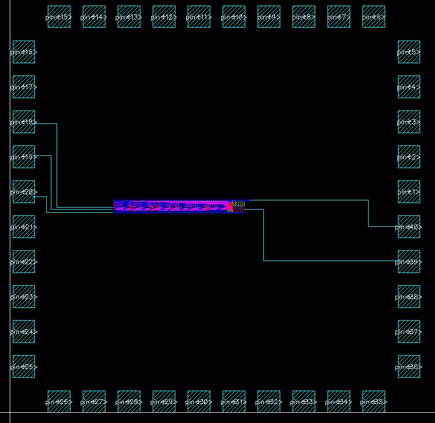
Chip Design
Below is the chip layout with the detector and buffer. The following are the pin assignments for the detector:
| Pin Number | Pin Name |
| pin<18> | clk |
| pin<19> | in |
| pin<20> | gnd |
| pin<39> | buff_out |
| pin<40> | vdd |
Schematic
Layout
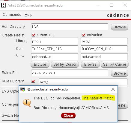
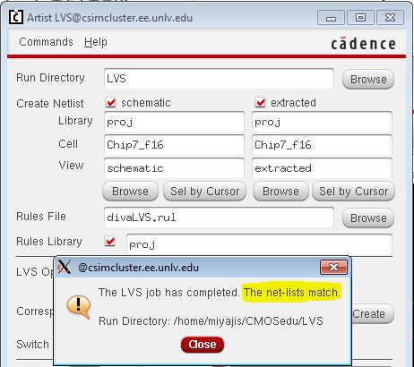
LVS
DRC

Here is the zip file: proj.zip
Return to Sharyn's Labs
Return to EE421L Labs