Lab 7 - EE 421L
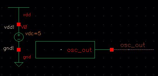
Symbol

Extracted

DRC

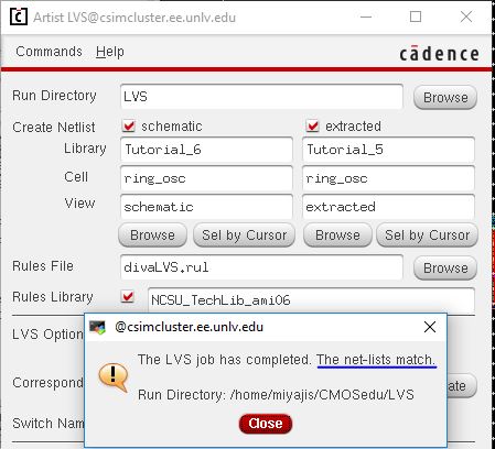
LVS
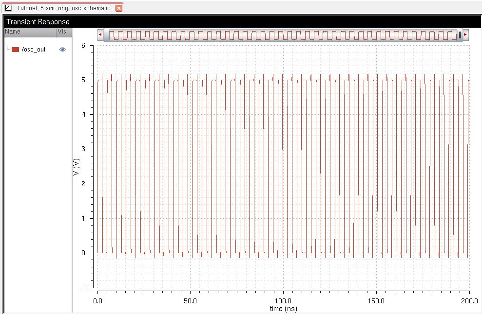
Simulation
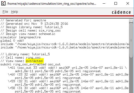
Netlist
Lab Work
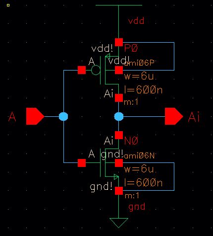
Symbol
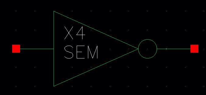
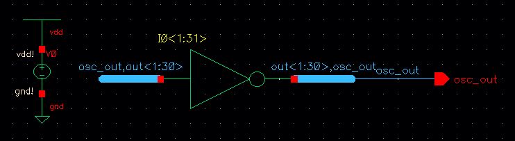
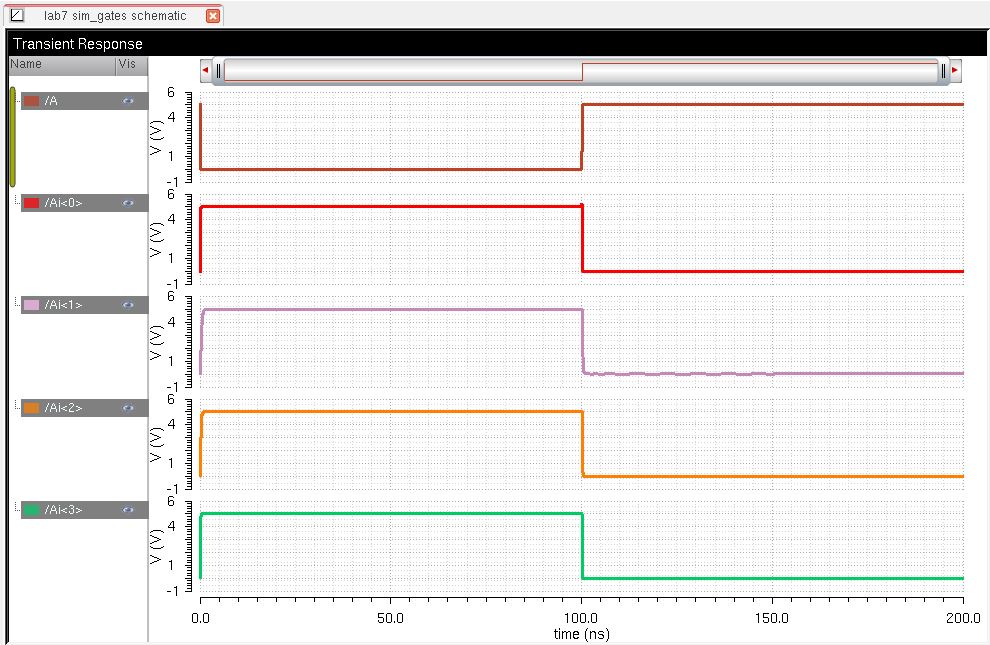
Using the 4-bit inverter, we test it to see if it is working properly by attaching different size capacitor loads to a different output bit to see how it affects the simulation.
Schematic of 4-Bit Inverter Simulation
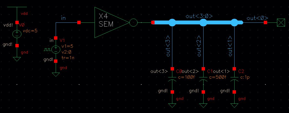
4-Bit Inverter Simulation
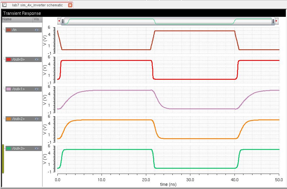
Based on the simulation, the bigger the capacitive load, the bigger the time delay. Both the rise and fall times increase as well as the capacitive load increases. If the capacitor is big, more charges can be stored; therefore, it is causing the voltage to take longer time to rise and fall.
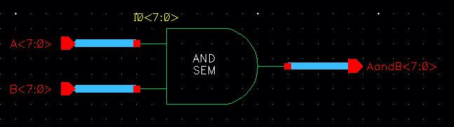
8-Bit NAND
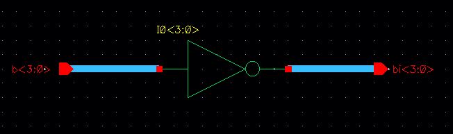
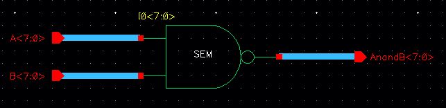
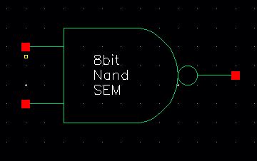
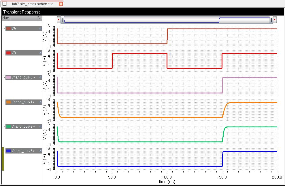
Now, we must create an 8-bit NAND gate by again using bus wires and by adding <7:0> to its pin names to represent the array of 8 bits. In order to do that, a single bit NAND gate must be created as shown below. Once the schematic is checked and saved and a symbol is created. Bus wires are attached witharrayed pins and the instance name of the NAND gate IO<7:0>. Once that is checked and saved, create another symbol as a representation of 8-bit NAND gate.
1-Bit NAND
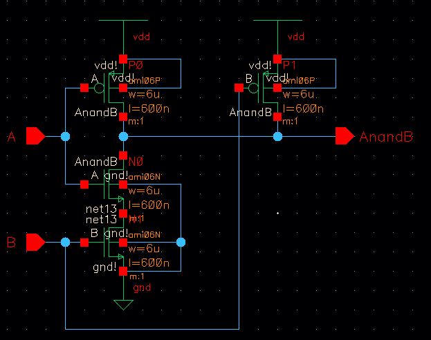
Schematic
Symbol
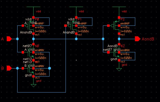
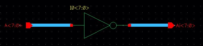
The same process is done for the inverter, NOR, AND, NAND, and OR gates.
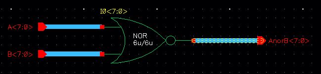
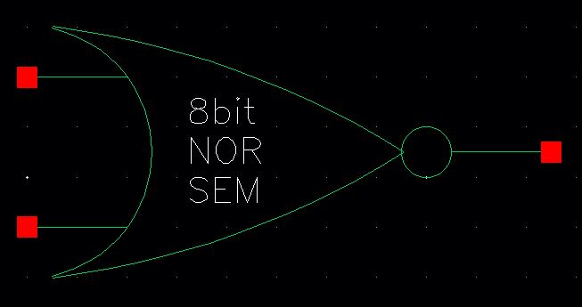
8-Bit NOR
1-Bit NOR
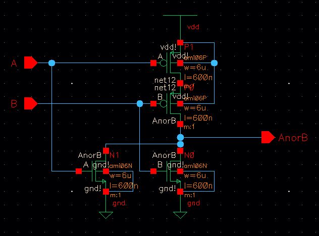
Schematic
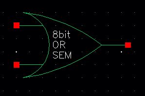
8-Bit OR
1-Bit OR
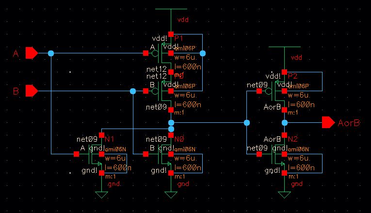
Schematic
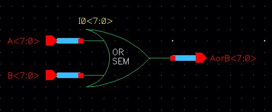
Symbol
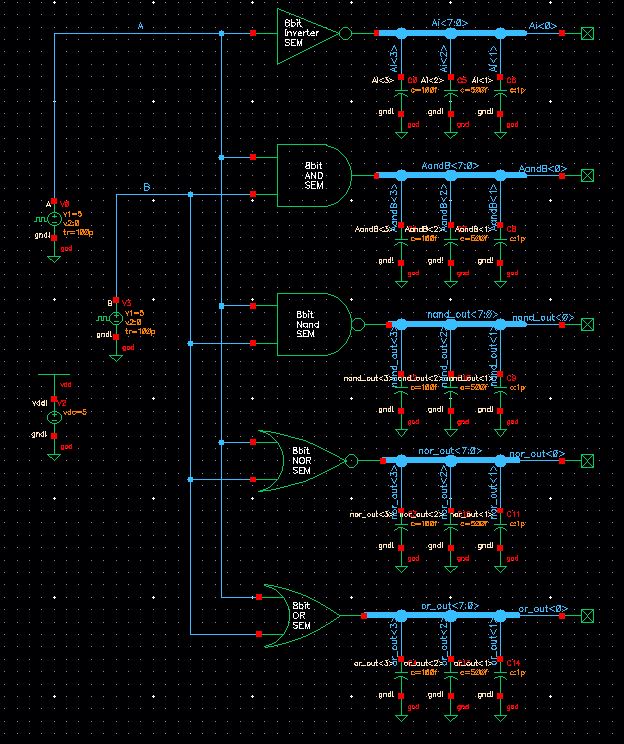
Gate Simulations
Once all 5 gates are created, the schematic below is created to see if the gates are working properly, which is similar as the one done for the 4-bit inverter.
Gate Schematic
8-Bit Inverter Simulation
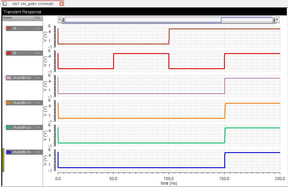
8-Bit AND Simulation
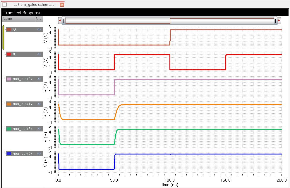
8-Bit NOR Simulation
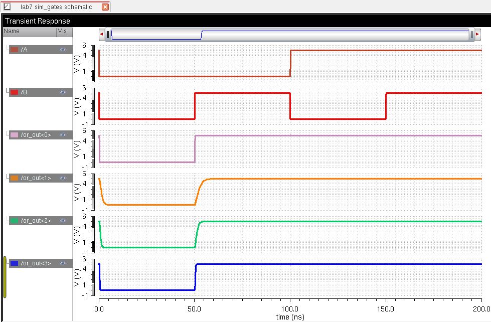
8-Bit OR Simulation
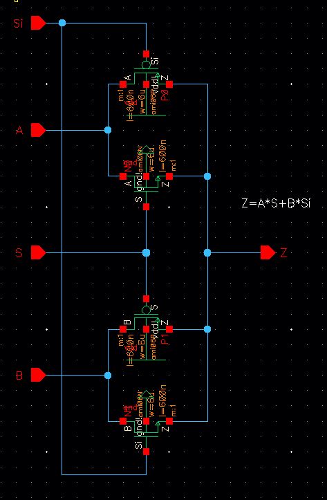
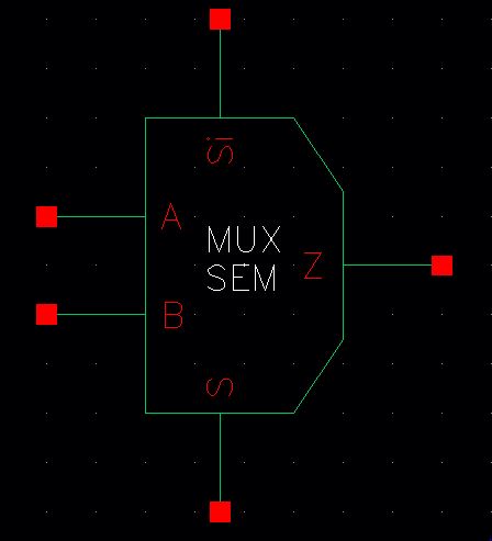
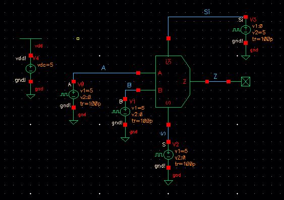
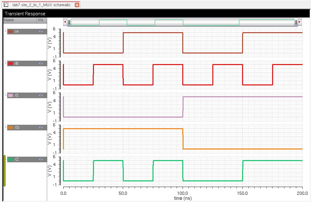
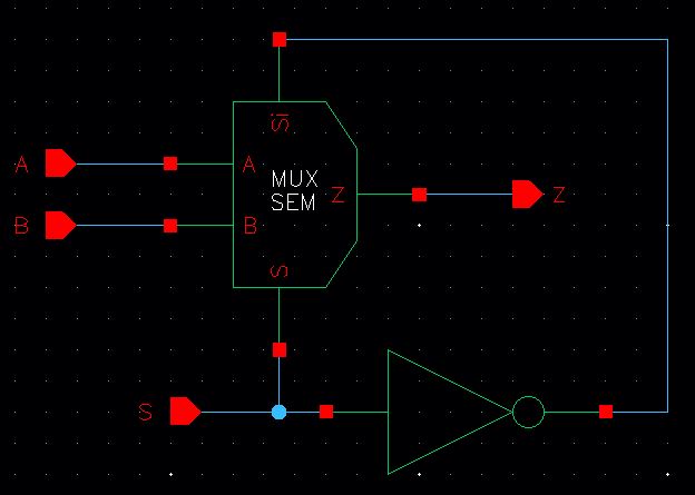
Next, a schematic of a 2-to-1 MUX is shown below and then created into a symbol, so it can be used for simulations. The output of the 2-to-1 MUX is dependent on the input of S because it causes the output to be either A or B as seen in the simulation.
2-to-1 MUX Schematic
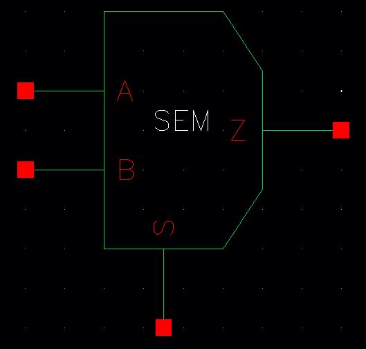
2-to-1 MUX Symbol
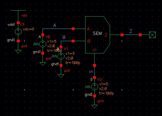
2-to-1 MUX Simulation Schematic
2-to-1 MUX with Inverter Schematic
2-to-1 MUX with Inverter Symbol
2-to-1 MUX with Inverter Simulation Schematic
2-to-1 MUX with Inverter Simulation
As you can see in the simulation, the inverter does not affect the results of the simulation; therefore, it does not matter whether or not the inverter is attached.
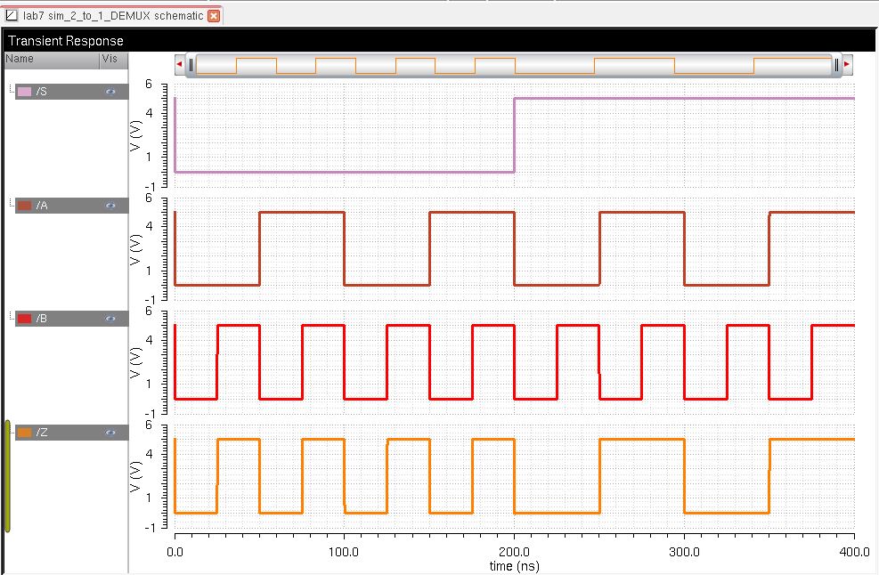
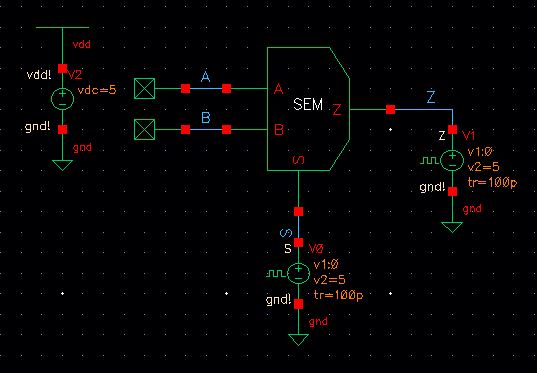
Using the modified 2-to-1 MUX, pulse voltage sources are attached to the pin Z and S, which are the new input pins, and pin A and B are being measured, which are the new output pins, to simulate a DEMUX.
2-to-1 DEMUX Simulation Schematic
2-to-1 DEMUX Simulation
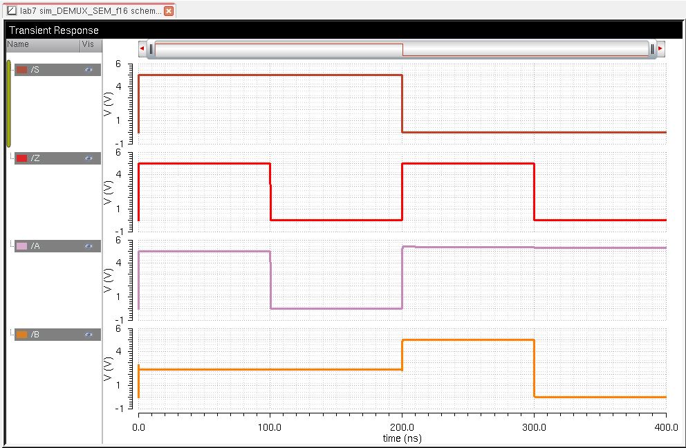
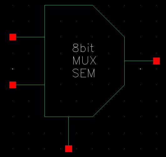
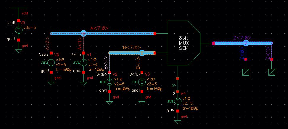
8-Bit 2-to-1 MUX
An 8-bit 2-to-1 MUX are created by again using bus wires and instance name to represent the arrays. Different pulse voltage sources are used to test if the 8-bit 2-to-1 MUX is working properly.
Schematic
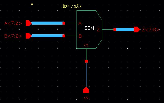
Symbol
Simulation Schematic
Simulation
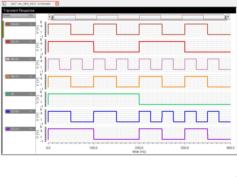
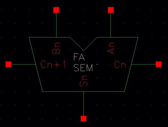
Figure 12.20 Full Adder
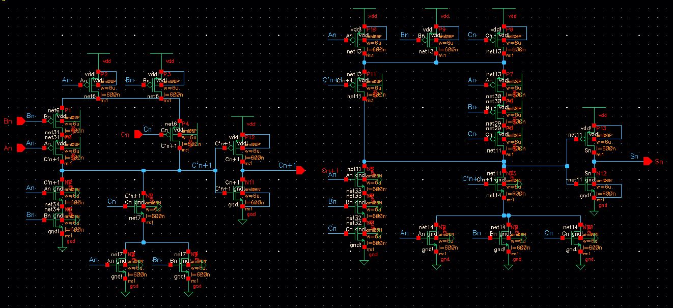
Symbol
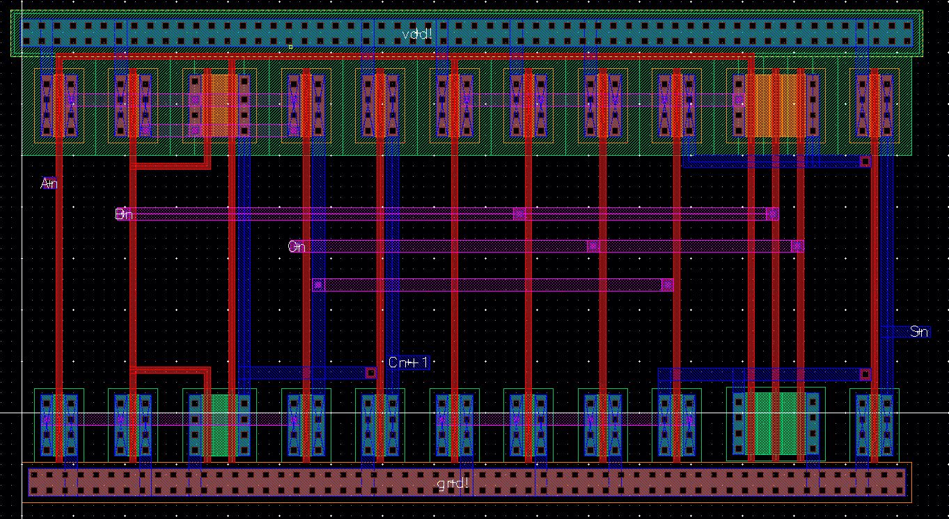
Layout
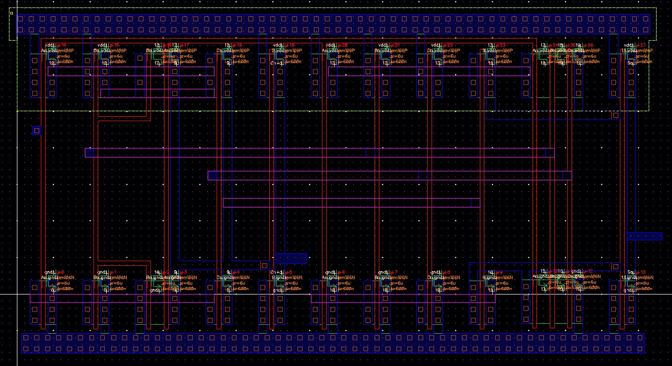
Extracted
DRC

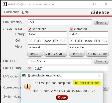
LVS
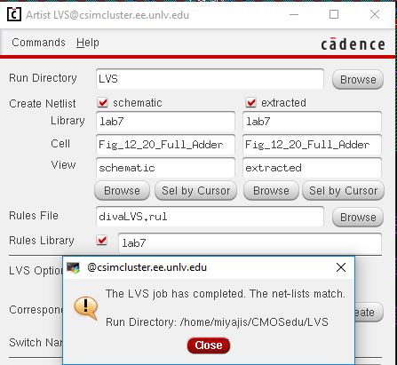
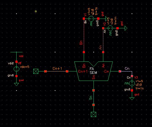
Once everything matches, the full adder is then tested out and has the same result as the full adder created in Lab 6.
Schematic
Simulation
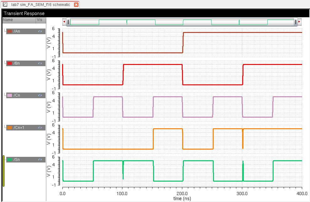
Truth Table
| An | Bn | Cn | Sn | Cn+1 |
| 0 | 0 | 0 | 0 | 0 |
| 0 | 0 | 1 | 1 | 0 |
| 0 | 1 | 0 | 1 | 0 |
| 0 | 1 | 1 | 0 | 1 |
| 1 | 0 | 0 | 1 | 0 |
| 1 | 0 | 1 | 0 | 1 |
| 1 | 1 | 0 | 0 | 1 |
| 1 | 1 | 1 | 1 | 1 |
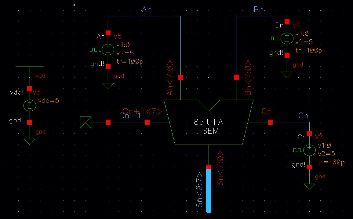
8-Bit Figure 12.20 Full Adder
Using the full adder that was just created, we will again use wire buses and instance name to create an 8-bit Full Adder. Once that is created, then we create a symbol and layout it out. When creating the 8-bit full adder, the first bit Cn+1 must connect to the second Cn, then the second but Cn+1 must connect to the third Cn, and so on and so forth, where the first Cn is an input and the last Cn+1 is the output.
Schematic
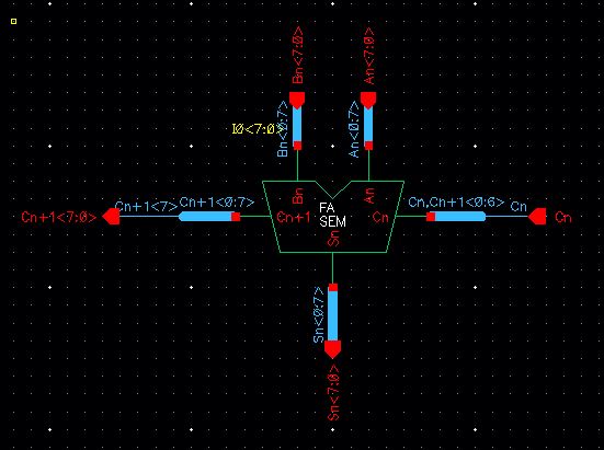
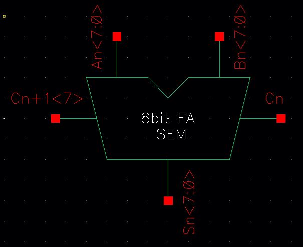
Symbol
Layout

Extracted

DRC

LVS
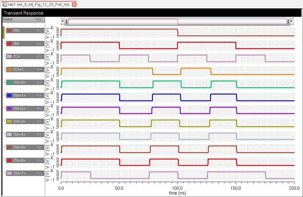
Once layout is DRCed, extracted, and LVS, then it can be tested out for simulation to see if it is properly working.
Simulation Schematic
Simulation
Here are the Lab 7 file: lab7.zip
Back-Up