Lab 4 - EE 421L
·
Back-up all of your work from the lab and the course.
·
Read through this lab before starting it.
·
Go through Tutorial 2 seen here.
·
In the simulations in this lab the body of all NMOS devices (the
substrate) should be at ground (gnd!) and the body of
all PMOS devices (the n-well) should be at a vdd! of
5V.
Lab
Description:
This lab will
include IV characteristics and layout of NMOS and PMOS devices in ON's C5
process.
Lab Report
should include:
·
IV curves of the NMOS and the PMOS
·
The layout of the NMOS and the PMOS
·
Layout of the NMOS and PMOS attached to 4 probe pads
First, I made
a new library and copied my files from tutorial 2 into that library. I
instantiate a nmos4 to make NMOS schematic, adding pins, made sure the body was
connected to gnd!, and then generated
symbol for it.


Figure 1 Figure
2
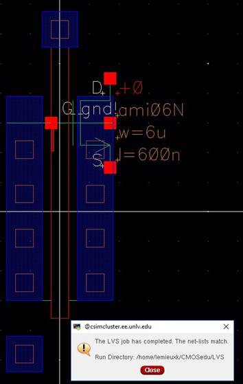
Next, I made
the NMOS layout, DRC’d it, extracted it, and made
sure it LVS’d with the schematic.


Figure 3 Figure
4

Figure 5
Generate 4
schematics and simulations (see the examples in the Ch6_IC61 library, but note
that for the PMOS body should be at vdd! instead of gnd!):
·
A schematic
for simulating ID v. VDS of an NMOS device for VGS varying from 0 to 5 V in 1 V
steps while VDS varies from 0 to 5 V in 1 mV steps. Use a 6u/600n
width-to-length ratio.
I copied the
NMOS from tutorial 2 into my library for lab 4 seen below. The parametric
analysis is sweeping VGS from 0V to 5V in 1V steps. The left picture is the
schematic while the right is the parametric analysis.


Figure 6 Figure
7
·
A schematic
for simulating ID v. VGS of an NMOS device for VDS = 100 mV where VGS varies
from 0 to 2 V in 1 mV steps. Again use a 6u/600n width-to-length ratio.
In the schematic below of the NMOS,
VDS was chanted to 100mV. In ADE I then change the component to V0 for VGS to
weep the parameter from 0V to 2V in 1V steps.
I am holding VDS constant and varying VGS. The results from the
simulation were as expected in the second picture below.

 Figure 8 Figure
9
·
A schematic
for simulating ID v. VSD (note VSD not VDS) of a PMOS device for VSG (not VGS)
varying from 0 to 5 V in 1 V steps while VSD varies from 0 to 5 V in 1 mV
steps. Use a 12u/600n width-to-length ratio.
Below is a
schematic of a 12u/600n(L/W) PMOS. By setting VSD from 0V to 5V and varying VSG
from 0V to 5V in 1V steps, the following parametric analysis results in the
second image.


Figure 10 Figure
11
·
A schematic
for simulating ID v. VSG of a PMOS device for VSD = 100 mV where VSG varies
from 0 to 2 V in 1 mV steps. Again, use a 12u/600n width-to-length ratio.
Using the same
PMOS, I am now holding the VSD at 100mV as seen in the schematic below. Now
sweeping VSG from 0V to 2V in 1mV steps the following IV curve simulation
results below. This simulation is similar to the characteristics of the NMOS.


Figure 12 Figure
13
Experiment 2:
·
Layout a
6u/0.6u NMOS device and connect all 4 MOSFET terminals to probe pads (which can
be considerably smaller than bond pads [see MOSIS design rules] and directly
adjacent to the MOSFET (so the layout is relative small).
I used the
NMOS_IV cell that was created in Tutorial 2 seen in Figure 3. I then
instantiated four probe pads and placed them appropriately. The probes were
connected to the NMOS using three different metals. I instantiated the
connections vias called m2_m1(connecting metal 1 and
metal 2) and m3_m2(connecting metal 2 to metal 3) as seen below in Figure 15.
I then DRC’s
the layout after all connections were made with zero errors seen in Figure 14.

Figure 14


Figure 15 Figure 16
Next, I created
a schematic by adding probes to the schematic of the NMOS I copied from
Tutorial 2. Seen below in Figure 17.

Figure 17
The LVS passed
and the netlists matched! Below in Figure 18 and Figure 19.


Figure 18 Figure
19
Experiment 3:
·
Layout a
12u/0.6u PMOS device and connect all 4 MOSFET terminals to probe pads.
I used the
PMOS created in Tutorial 2 (Figure 21) to create a layout for a 12u/0.6u
device. The same procedure was used for the PMOS as before that was used with
the NMOS. Connected three different metals with different vias
to reduce resistance between contact layers by instantiating m2_m1 and
m3_m2(also in Figure 21).
The layout was
DRC’s with zero errors seen below in Figure 20.

Figure 20

Figure 21

Figure 22
Again, I copied my PMOS schematic I made from Tutorial 2 and added
probes to it as seen in Figure 23.

Figure 23
I then LVS’s the extracted and schematic view successfully (Figure
24 and Figure 25).


Figure 24 Figure
25
Conclusion
In lab 4, we designed a NMOS and PMOS schematics and layouts using
the C5 process. They resulted in DRC and LVS verifications and similar
characteristics in simulations for both NMOS and PMOS.