Project – EE421L
Kristal Lemieux
30 Nov 2016
For the lab, I built a
detector. This will need an inverter, 6 D Flip-Flops, and a 6 input NAND.
First I made the inverter. Seen
below are the schematic view and symbol for it.


The layout and extracted
layouts for the inverter.


The layout DRC and LVS for
schematic and extracted.


The edge triggered D Flip-Flop
and 6-input NAND were next.
The D Flip-Flop takes a value
in sequence by the rising edge of the clock cycle.

Symbol for D Flip-Flop

Simulation for D Flip-Flop


The outputs respond to input D
whenever the clock is high, for however long it remains high.
When the enable signal falls
back to a low state, the circuit remains latched.
The clock only responds to the
D input during that brief moment of time when the enable signal changes, or
transitions, from low to high.
This is known as positive
edge-triggering.
6-Input NAND Schematic and
Symbol


Layout and Extracted Layout of
6-Input NAND


DRC and LVS of 6-Input NAND


Finally, the detector circuit.
Again, this consists of the 6-Input NAND and 6 D Flip-Flops.

Detector Symbol

Layout of the Detector Circuit

Zoomed in on part of the
Detector
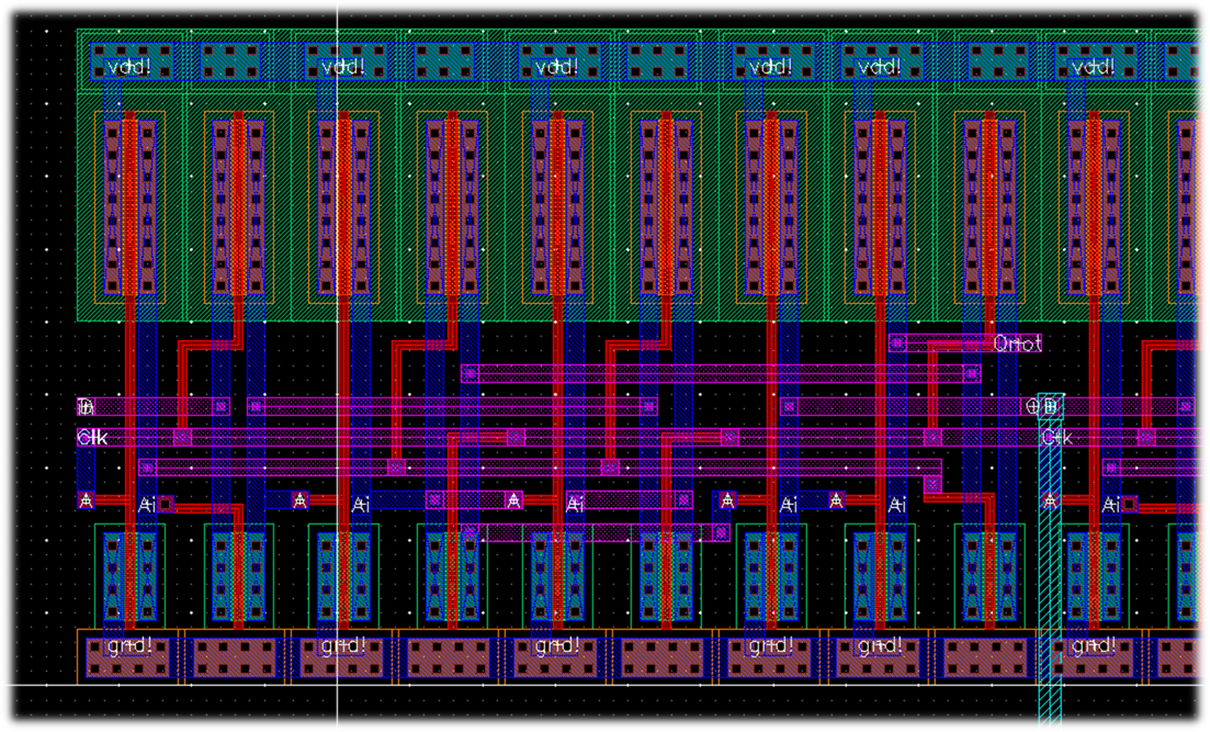
Where D Flip-Flops were
connected to Layout of NAND

DRC of Detector with zero
errors

Extracted View of Detector

LVS for Detector

Schematic for Simulating
Detector

The D Flip-Flops take the value
on the rising edge.
Detector circuit outputs high
when the sequence 101011 is inputted as shown below.
Simulations to show Detector is
working


Project lab
files can be accessed here.