Lab 4 - ECE 421L 

Authored by Antanasia Jones

jonesa20@unlv.nevada.edu


9/28/16


In this lab I had to make a schematic, symbol and layout of an NMOS and PMOS device. I then had to create circuit using the symbols of the devices and simulate the circuit by sweeping the different voltages, VGS and VDS for the NMOS and VSG and VSD for the PMOS. 


Initially I had to generate 4 schematics, 2 for the NMOS device and 2 for the PMOS device. 


Using the examples presented in Tutorial 2 and the example from the Ch6_IC61 library, I was able to generate the schematic for the NMOS and PMOS devices. I then generated circuits using the symbols of the 6u/600n NMOS and 12u/600n PMOS schematics which were used for simualtions. 


The first simulation showed ID v. VDS where VGS varied from 0 to 5V in 1V steps and VDS varied from 0 to 5V in 1mV steps, where VDS and VGS are repesented by voltage sources. To sweep VDS I had to make a dc analysis and a linear sweep of V1 in the circuit. To sweep VGS, I had to do a parametric analysis where VGS was selected as a variable to be sweeped. Below is the NMOS circuit and the simulation results. 


NMOS_circuit1.jpg

                    NMOS circuit to sweep VGS and VDS 

 sweep_vgs_vds.jpg

                                 Simulation results, ID v. VDS, of NMOS circuit, sweep of VGS and VDS from 0 to 5V


For the second simulations there was a similar process except that VDS = 100mV which meant I would only sweep VGS, having VGS vary from to 2V in 1mV steps. Below is the circuit and simulation results. 


NMOS_circuit_100mV.jpg

                    NMOS circuit VDS=100mV, sweep VGS


sweep_vgs.jpg

                                                  Simulation results, ID v. VGS,  of NMOS circuit,VDS = 100mV sweep VGS from 0 to 2V


The third simualtion was had the same process as the first simulation, just with a the circuit generated for the PMOS device and instead of VGS and VDS it was VSG and VSD.For this simulation VSG varied from 0 to 5V in 1V steps and VSD varied from 0 to 5V in 1mV steps. Circuit and simulation results shown below. 


PMOS_circuit1.jpg
                     PMOS circuit sweep VSD and VSG
   
sweep_vsg_vsd.jpg
                                                    Simulation results, ID v. VSD, of PMOS circuit, sweep VSD and VSG from 0 to 5V
 

For the fourth simulation VSD = 100mV and VSG was varied from 0 to 2V in 1mV steps. Circuit and simulation results shown below. 


PMOS_circuit_100mV.jpg

                                  PMOS circuit VSD=100mV, sweep VSG
   

 sweep_vsg.jpg

                                                           Simulation results, ID v. VSG, of PMOS circuit, VSD=100mV sweep VSG


I then created layouts of the 6u/600n NMOS and 12u/600n PMOS schematics connecting the terminals of the NMOS and PMOS to probe pads and created an extracted view of each layout. 


NMOS_layout_zoom.jpg         NMOS_layout.jpg 

                                 NMOS Layout                                                                           NMOS layout with probe pad connections 


PMOS_layout_zoom.jpg         PMOS_layout.jpg 

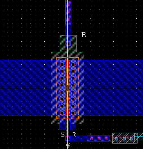
                                 PMOS Layout                                                                                  PMOS layout with probe pad connections 


I performed a DRC on the layouts to test for errors. 


NMOS_drc.jpg            PMOS_drc.jpg

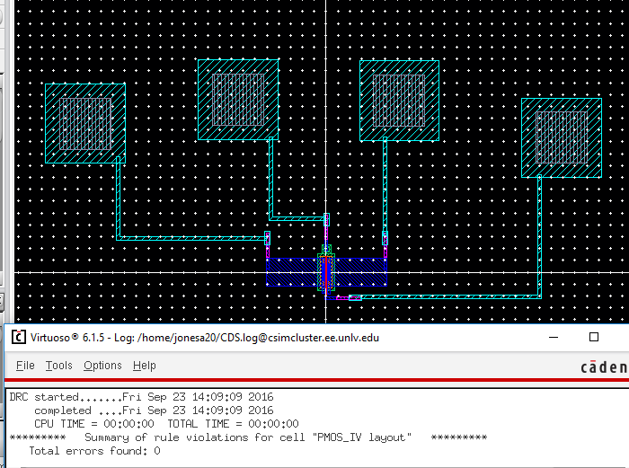
                                   NMOS DRC Test                                                                                                            PMOS DRC Test

Afterwards I revised the schematics of the NMOS and PMOS devices, connecting the terminals to probe pad symbols. I then performed LVS comparing the schematic of the NMOS/PMOS to the extracted view of the NMOS/PMOS. 


NMOS_schematic.jpg

                       NMOS Schematic with probe pad connections
   

NMOS_LVS.jpg

                                            LVS for NMOS schematic and NMOS layout 


PMOS_schematic.jpg 

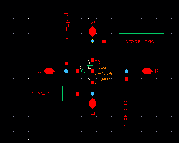
                   PMOS schematic with probe pad connections 


PMOS_LVS.jpg

                                             LVS for PMOS schematic and PMOS layout

Return to EE 421L labs