Lab 2 -
ECE 421L
Authored
by Tyler Huddleston, huddle10@unlv.nevada.edu
9/14/2016
In
this lab I designed a 10-bit Digital to Analog Converter (DAC) using
Cadence. I implemented the schematic and symbol, following the
procedures outlined in Tutorial 1.
I calculated the resistance and time delay of the DAC driving a
load and confirmed my calculations with transient analysis.
Pre-lab work
The prelab required adding the lab2 project to my design libary by:
1. downloading the lab2.zip file
2. uploading the lab2.zip file to my CMOSedu design directory
3. unzipping the project
4. adding the defintion "DEFINE lab2 $HOME/CMOSedu/lab2" to my cds.lib
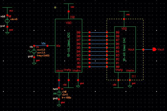
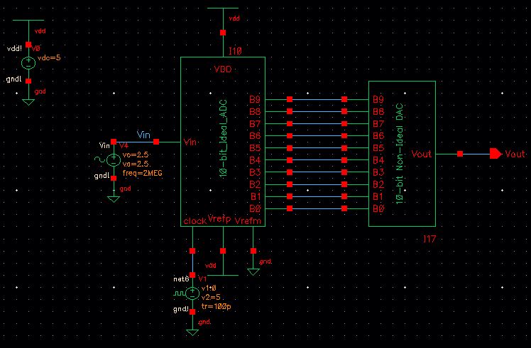
The lab2 project contains sim_Ideal_ADC_DAC, which is a design of an ADC to DAC with a sinusoid input.
Simulating this design involved:
1. Opening the ADE: Launch -> ADE L
2. Loading the spectre state: Session -> Load State -> Cellview
3. Clicking "Netlist and Run" (the green button)
Changing the line color: right click name -> Color -> color
Changing the line style: right click name -> Style -> style
Changing the plot background: right click plot -> Graph Properties -> Background Color
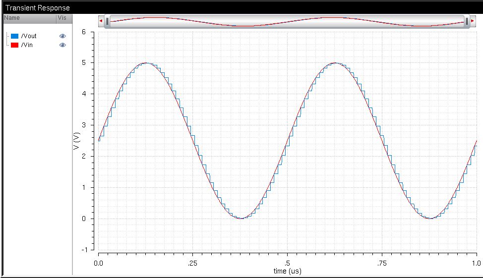
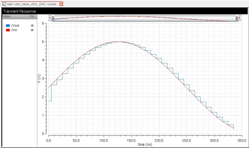
The simulation plot shows the smooth, analog sinusoid input in red and the staircased digital output in blue. The
sinusoid signal is first input to the ADC, which converts the analog
voltage to a 10-bit digital signal (or a continuous to discrete
signal). The digital signal only changes when the analog voltage
reaches certain levels and is held constant until the next level is reached, which is why the digital signal is staircased.
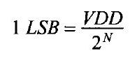
The least significant bit (LSB) is the lowest amount of voltage required to increment the digital signal and is determined by
Lab Work
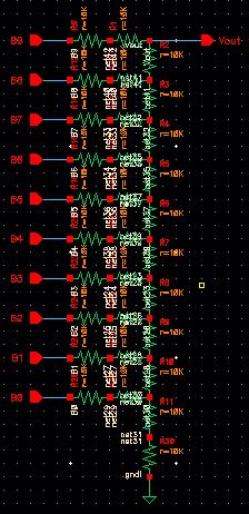
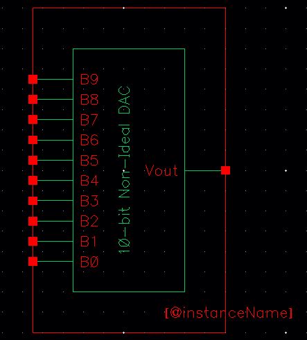
10-bit DAC with 10k resistors.
This design is the R-2R ladder network described on page 971. The inputs are pins B9-B0, with output Vout.
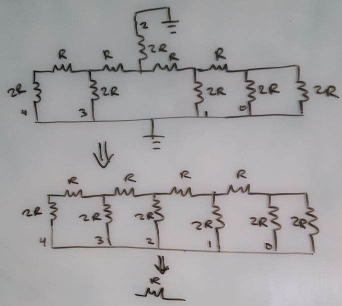
Thevenin's
theorem can be applied to determine the Thevenin/output resistance.
Thus, all pins (voltage sources) are set to ground and the
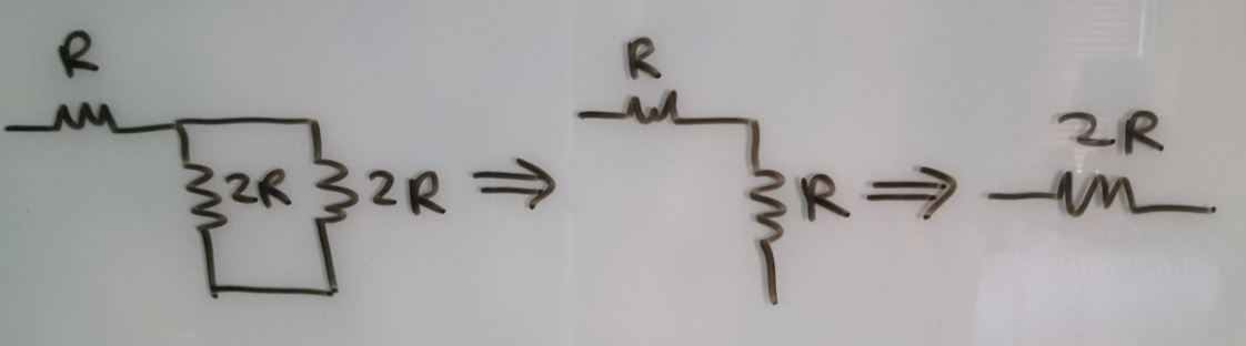
resistor network can be simplified by combining resistors in parallel
and series. The ouput resistance is simply R. The 5-bit
R-2R ladder network is shown below.
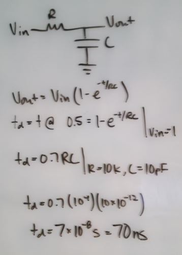
The time delay for driving a capacitive load
The circuit can be simplified when the most significant bit (B9) is high and the rest are grounded as:
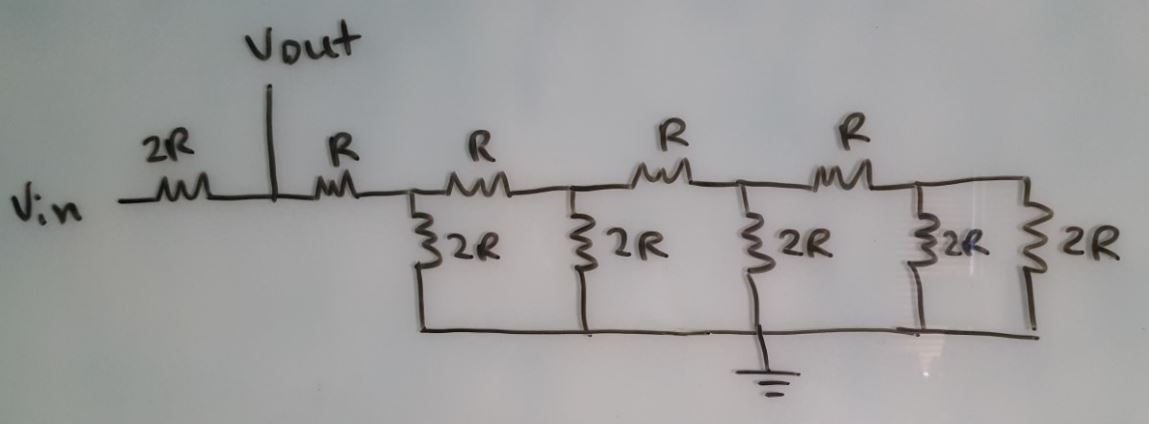
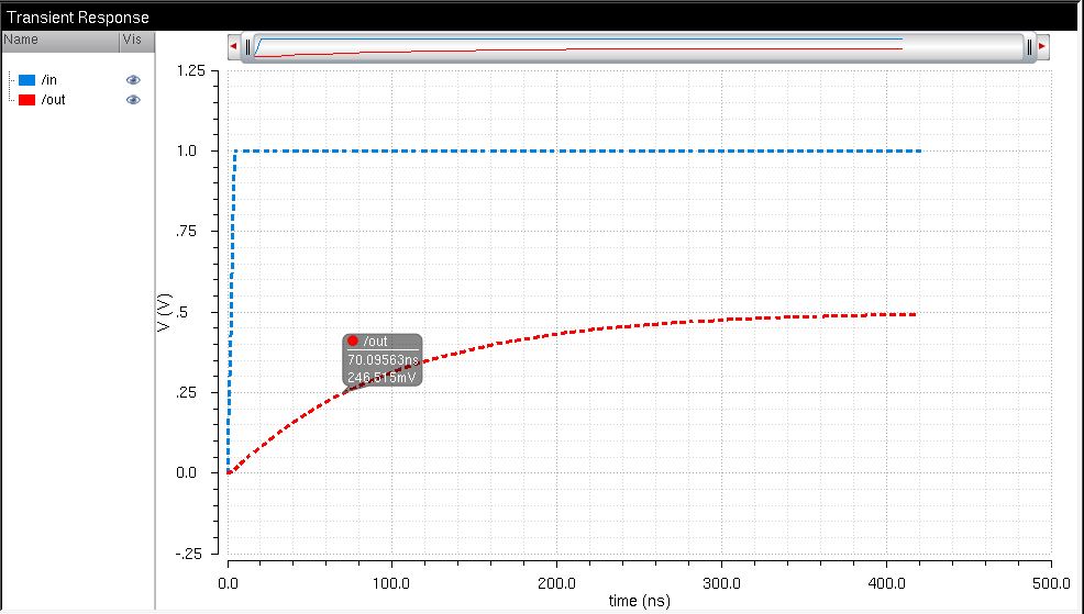
With output resistance R = 10k and capacitive load C = 10pF, the DAC circuit becomes an RC circuit with time delay of 70ns.
Vout,max = 0.5V for Vin = 1V and td = 70ns was verified by simulation:
To
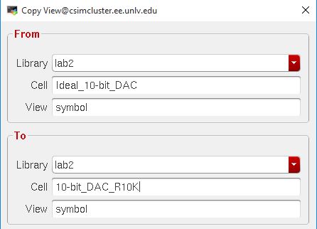
create the symbol for my 10-bit DAC, I copied the ideal_10-bit_DAC
symbol and modified it. I removed the connections that were not
needed on my schematic (VDD, Verfp, or Vrefm).
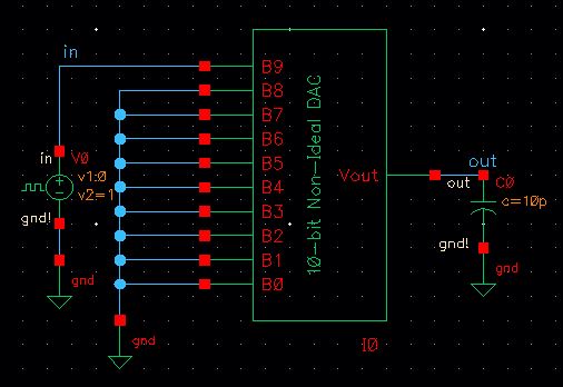
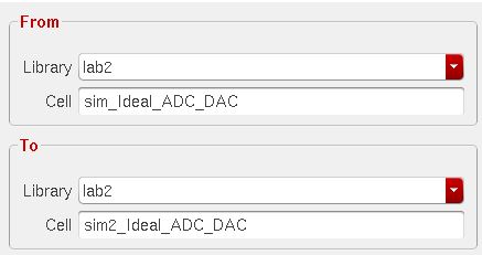
To test my schematic and symbol, I copied the sim2_Ideal_ADC_DAC schematic, removed the ideal_10-bit_DAC,
and inserted my 10-bit_DAC in its place. Then, ran the simulation
to verify that it works just as before.
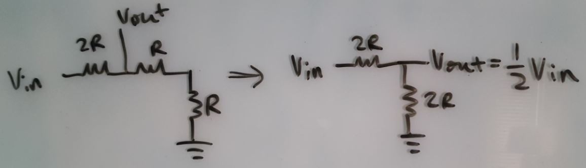
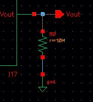
When
this circuit drives a purely resistive load, the output voltage Vout is
divided between the DAC resistance (R = 10k) and the load. When
the load is equal to the output resistance, then the output voltage
will be half of the input voltage as shown below.
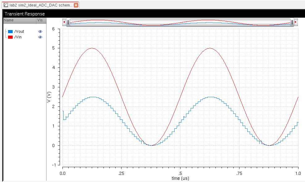
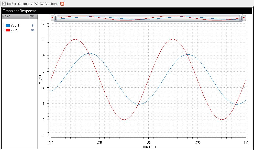
When
the load is capacitve the digital output is smoothed by the fast RC
delay so that it appears continuous. The magnitude of the output
is reduced inversely proportional to the input frequency. With an
imaginary impedance for the load, the output is out of phase with the
input as shown below.
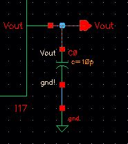
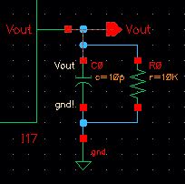
When the load is resistive and capacitive the output
voltage is divided across the DAC resistance and load resistance.
The output signal is smoothed by the time delay of charging and
discharging the capacitor. The output is alsoout of phase with the input due to the capacitance.
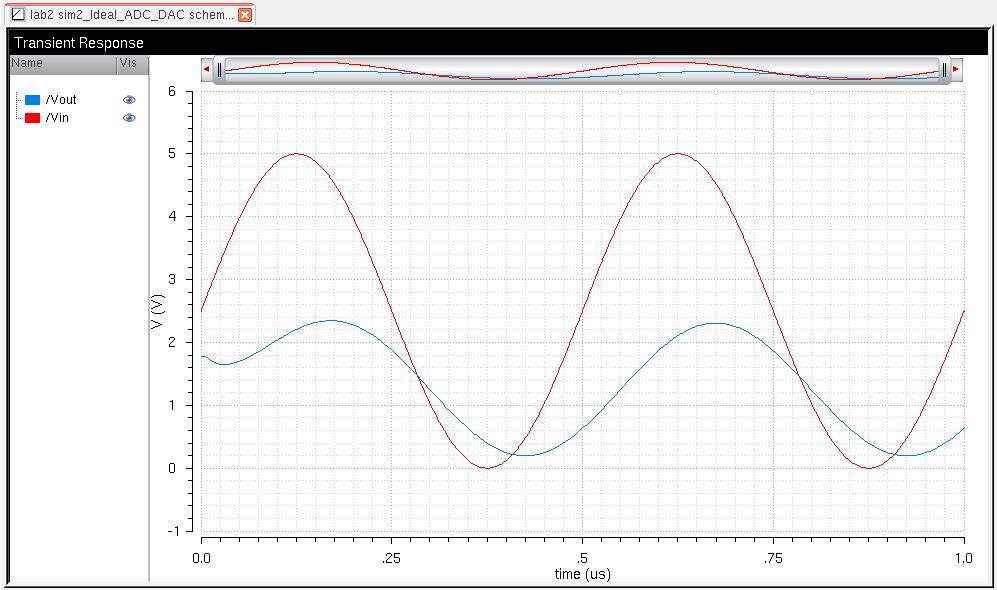
When the input resistance from the switches is much larger than R, the magnitude of the output voltage becomes much smaller as the output voltage is divided over the large input resistance and the output resistance of the DAC.
Return
to EE 421L Labs
Return to my Labs Index