Lab 7 - EE 421L
Digital Integrated Circuit Design
Garnerj5@unlv.nevada.edu
22 October 2016
Return to: J.Garner EE421 Labs
Pre-lab work
- Back-up
all of your work from the lab and the course.
- Go
through Tutorial 5 seen here.
- Read
through the entire lab before starting it.

Experiment 1:
Using a single
input inverter, create a 4Bit Inverter using Cadence Tools.
Schematic

Symbol

Simulation Schematic

Simulations

Question: Show,
in your lab report, how a capacitive load influences the delay and rise/fall
times.
From the figure
above we can see that capacitive loads influence simulation characteristics,
with higher capacitance leading to “smoother” curves. High capacitance causes
rise/fall times, and the delay to rise (Pink vs Green). The green line was the smallest
capacitance used which shows an almost perfect simulation compared to the no
load output (Red).
Experiment 2:
Create schematics and symbols for an 8-bit input/output array of:
NAND, NOR, AND, inverter, and OR gates. Provide a few simulation examples using
these gates.
In the following
schematics and symbols I used previously created NAND/NOR/NOT gates to
implement the AND and OR gates by simply putting a
NAND and NOT gate in series we get a AND gate. The same can be said for a OR
gate.
NOT GATE:
Schematic (Basic NOT)

NOTx8 Schematic

NOTx8 Symbol

NAND GATE:
Schematic (Basic NAND)

NANDx8 Schematic

NANDx8 Symbol

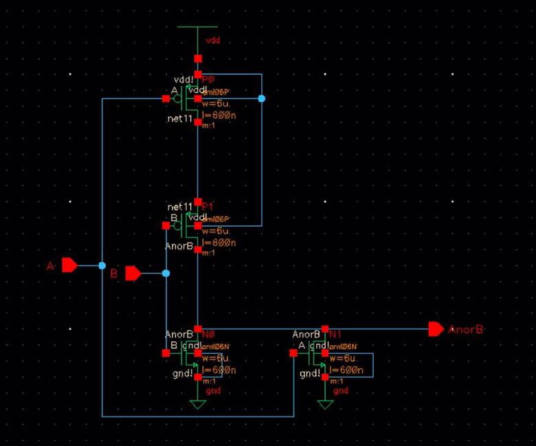
NOR GATE:
Schematic (Basic NOR)

NORx8 Schematic

NORx8 Symbol

AND GATE:
ANDx8 Schematic

ANDx8 Symbol

OR GATE:
ORx8 Schematic

ORx8 Symbol

LOGIC GATE
SIMULATIONS:

|
A |
B |
NOT (A) |
AND |
OR |
NAND |
OR |
|
0 |
0 |
1 |
0 |
0 |
1 |
1 |
|
0 |
1 |
1 |
0 |
1 |
1 |
0 |
|
1 |
0 |
0 |
0 |
1 |
1 |
0 |
|
1 |
1 |
0 |
1 |
1 |
0 |
0 |
High Capacitance

Medium Capacitance

Low Capacitance

Next examine the following schematic.
2:1 Mux Schematic

2:1 Mux Symbol

2:1 Mux
Simulation

This is the schematic of a 2-to-1 DEMUX/MUX (and
the symbol).
Simulate the operation of this circuit using Spectre
and explain how it works.
This simulation shows that the output Z, is
selected by signal S. Signal S, when it is low will choose to output signal B,
and when it is high it will output signal A. Si is just the inverse of signal
S.
Make sure to show, using simulations, how the
circuit can be used for both multiplexing and de-multiplexing.
2:1 Demux Schematic

2:1 Demux Symbol

2:1 Demux Simulation

This simulation shows the operation of DEMUX.
Here we see that Z is the input signal and S is the control signal to control
the output. When S is high we are outputting Z to signal A and signal B could
be anything. When S is low we are outputting Z to signal B and signal A could
be anything.
Create an 8-bit wide word 2-to-1 DEMUX/MUX
schematic and symbol.
Include an inverter in your design so the cell only needs one select input, S
(the complement, Si, is generated using an inverter).
Use simulations to verify the operation of your design.
8bit 2:1 Demux/Mux Schematic

8bit 2:1 Demux/Mux Symbol

8bit 2:1 Demux/Mux Simulation

The 8bit design shows that when signal S is
high, we are outputting both signal Z<0> and Z<1> from signal
A<0> and A<1> respectively. When S goes low, we are outputting from
signals B<0> and B<1>.
Finally, draft the schematic of the full-adder seen in Fig. 12.20 using 6u/0.6u
devices (both PMOS and NMOS).
Create an adder symbol for this circuit (see the symbol used in lab6).
Full Adder
Schematic Part A

Full Adder
Schematic Part B

Full Adder Symbol

Full Adder Simulation

Full Adder Layout

Full Adder DRC

Full Adder LVS

Use this symbol to draft an 8-bit adder
schematic and symbol.
For how to label the bus so the carry out of one full-adder goes to the carry
in of another full-adder review the ring oscillator schematic discussed in
Cadence Tutorial 5.
Simulate the operation of your 8-bit adder.
8bit- Full Adder
Schematic

8bit- Full Adder
Symbol

8bit- Full Adder Simulation
Schematic

8bit- Full Adder Simulation Results

Lay out this 8-bit adder cell (*note* that this is the only layout required in
this lab).
Show that your layout DRCs and LVSs correctly.
8bit- Full Adder
Layout

8bit- Full Adder
DRC

8bit- Full Adder LVS
