Lab 5 - EE 421L
Digital Integrated Circuit Design
Garnerj5@unlv.nevada.edu
1 October 2016
Return to: J.Garner EE421 Labs
Design, layout, and simulation of a CMOS
inverter
Pre-lab work
- Back-up all of your work from the lab and the course.
- Go through Tutorial 3 seen here.

Lab work
- Draft schematics, layouts, and symbols for two
inverters having sizes of:
- 12u/6u (= width of the PMOS / width of the
NMOS with both devices having minimum lengths of 0.6u)
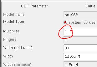
- 48u/24u where the devices use a
multiplier, M = 4 (set along with the width and length of the MOSFET, image), as
seen below
- Example
layouts are seen below.
- Notice
that power is run on the top of the cell via metal1 and ground is run on
the bottom of the cell also via metal1
- Power
(vdd!) is connected to the n-well using the ntap cell
- Ground
(gnd!) is connected to the p-substrate using
the ptap cell
- Running
power and ground with a single row of contacts, instead of 2 as seen
below, is fine to reduce layout size
- Your
schematics should have two pins, e.g., A and Ai
- Your
layouts should have 4 pins: A, Ai, vdd!, and gnd! (note how lowercase letters are used for
power and ground)
- Your
lab reports should document your efforts and results including showing
that the extracted layouts and schematics LVS correctly
- Zip
up these cells in a directory call lab5_rjb.zip (last two or three
letters are your initials) and link to your lab report
12u/6u Inverter
Schematic

12u/6u Inverter
Symbol

12u/6u Inverter
Layout

12u/6u Inverter
DRC

12u/6u Inverter
LVS

48u/24u Inverter
Schematic

48u/24u Inverter
Symbol

48u/24u Inverter
Layout

48u/24u Inverter
DRC

48u/24u Inverter
LVS

- Using
SPICE simulate the operation of both of your inverters showing each
driving a 100 fF, 1 pF, 10 pF, and 100 pF
capacitive load
- Comment,
in your report, on the results
12u/6u Inverter

48u/24u Inverter

We can see from these simulations for both
inverters that as you increase the capacitor value, the output will invert at a
much slower rate. (See light blue trace in 12u/6u and in 48u/24u Inverters which
are 100p, while the red trace in both simulations are 100f)
- Use UltraSim
(Cadence's fast SPICE simulator for larger circuits at the cost of
accuracy) and repeat the above simulations
- Use Setup ->
Simulator/Directory/Host and select UltraSim as
seen below
- You'll also have to
point to the MOSFET models again as seen below
- Note that UltraSim only performs transient simulations
(not AC, Noise, DC, operating point, etc.)
- Not knowing this last
item will lead to wasted time if trying to use UltraSim
exclusively for simulations
12u/6u Inverter

48u/24u Inverter

When analyzing the UltraSim
simulations vs the specter simulations we can see that they are very similar.
They are similar because UltraSim is still accurate
for smaller, less complex circuits.