

Lab 4 - ECE 421L
Pre Lab
As always for the prelab we were required to backup all of the files from both the lab and the course. Once this is done, the prelab instructed us to complete Tutorial 2. This tutorial introduced us to the layout and simulation of PMOS and NMOS transistors. The lab also introduced us to the ability to perform a simulation based on the extracted view as well as showing us how to run a parametric analysis. All of these things would then be used in the lab for this week.
Lab Report
The first part of the lab was to generate four schematics and simulations that each test ID against a varying voltage.
1) ID v. VDS of a NMOS device
This first simulation has us vary VGS from 0 to 5V in 1V steps while also varying VDS from 0 to 5V by 1mV steps
2) ID v. VGS of a NMOS device
This second simulation has us vary VGS from 0 to 2V in 1mV steps while keeping VDS at 100mV


3) ID v. VSD of a PMOS device
The third simulation seen below had us vary VSG from 0 to 5V in 1V steps while VSD varied from 0 to 5V in 1mV steps


4) ID v. VSG of a PMOS device
The final simulation had us set VSD = 100mV while VSG varied from 0 to 2V in 1mV steps


The next part of the lab required us to layout both an NMOS device. The terminals of this device had to be connected to 4 probe pads.
The dimensions of this NMOS device are: L = 0.6um and W = 6um.
Layout a 6u/0.6u NMOS device and connect all 4 MOSFET terminals to probe pads
We first begin this layout by creating a layout of the NMOS device.

This NMOS device is what will be used with the probe pads. The terminals of this NMOS device will each be connected to its own individual probe pad. The layout of this can be seen below.

The following image is a close up view of the NMOS device in the above layout.

The extracted view of the NMOS device is seen below. This extracted view is used with the LVS test to ensure that both the netlist of the schematic and match.

In
addition to laying out the NMOS device with the probe pads attached, we
were also asked to create a schematic of the NMOS device with probe
pads attached. This schematic and its symbol can be seen below.


Since both the schematic and layout for the probe were created, we are now free to run the DRC and LVS checks for the NMOS device.


As we can see, the DRC returned no errors and the LVS states that the schematic and layout match.
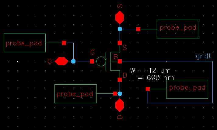
Layout a 12u/0.6u PMOS device and connect all 4 MOSFET terminals to probe pads
The layout of this device follows the same steps as the NMOS created above. The only difference is that a PMOS device is used instead of the NMOS device.
The PMOS device used for this layout and schematic can be seen below. Its dimensions are: L = 0.6um and W = 12um.

This PMOS device was used in the layout seen below. It is connected to four probe pads.

The following image is a close up of the PMOS device in the layout.


The schematic and symbol for a PMOS device connected to four probe pads can be seen below.

The DRC and LVS of the PMOS device returned no errors and are able to seen in the images below.

