Lab 6: Design, Layout, and Simulation of a CMOS NAND gate, XOR gate, and Full-Adder - EE 421L
Authored By: Joey Yurgelon
Email: yurgelon@unlv.nevada.edu
October 3rd, 2015
Pre-lab Work:
- Back-up all of your work from the lab and the course.
- Go through Cadence Tutorial 4 seen here.
- Read through the lab in its entirety before starting to work on it
Lab Description:
- Students
will simulate and layout CMOS NAND, XOR, and Full-Adder in the C5 process.
Lab Requirements:
- Draft
the schematics of a 2-input NAND gate (Fig. 12.1), and a 2-input XOR
gate (Fig. 12.18) using 6u/0.6u MOSFETs (both NMOS and PMOS)
- Create layout and symbol views for these gates showing that the cells DRC and LVS without errors
- ensure
that your symbol views are the commonly used symbols (not boxes!) for
these gates with your initials in the middle of the symbol
- ensure all layouts in this lab use standard cell frames that snap together end-to-end for routing vdd! and gnd!
- use a standard cell height taller than you need for these gates so that it can be used for more complicated layouts in the future
- ensure gate inputs, outputs, vdd!, and gnd! are all routed on metal1
- Use cell names that include your initials and the current year/semester, e.g. NAND_jb_f19 (if it were fall 2019)
- Using Spectre simulate the logical operation of the gates for all 4 possible inputs (00, 01, 10, and 11)
- comment on how timing of the input pulses can cause glitches in the output of a gate
- Your html lab report should detail each of these efforts
- Using these gates, draft the schematic of the full adder seen below
- Create a symbol for this full-adder (example)
- Simulate, using Spectre, the operation of the full-adder using this symbol
- Layout the full-adder by placing the 5 gates end-to-end so that vdd! and gnd! are routed
- full-adder inputs and outputs can be on metal2 but not metal3
- DRC and LVS your full adder design
- ALL OF THE DESIGN FILES ASSOCIATED WITH THIS LAB CAN BE FOUND HERE.
Pre-Lab:
Exercise #1: Go through Cadence Tutorial 4.
- The below layout and schematic were generated while going through Tutorial 4.
Experimental Results:
Exercise #1: Draft
the schematics of a 2-input NAND gate (Fig. 12.1), and a 2-input XOR
gate (Fig. 12.18) using 6u/0.6u MOSFETs (both NMOS and PMOS)
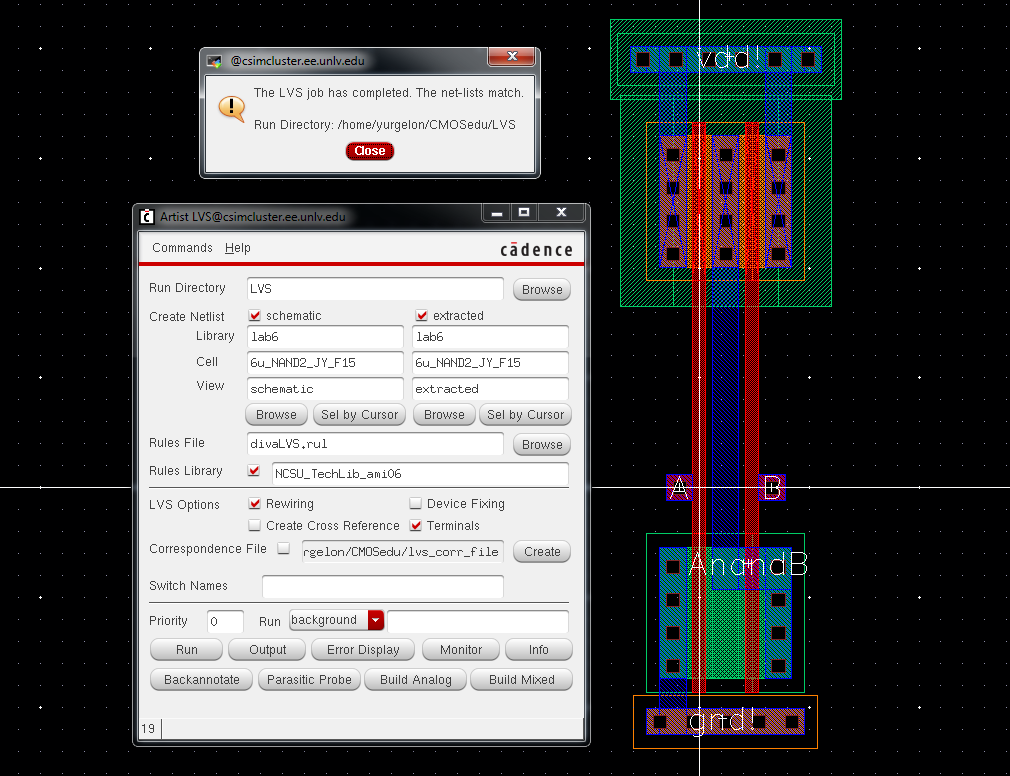
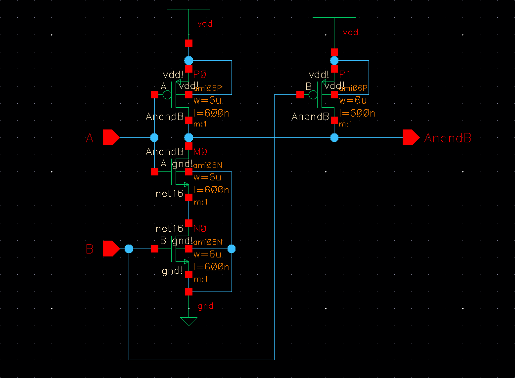
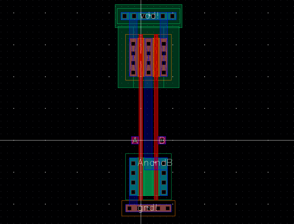
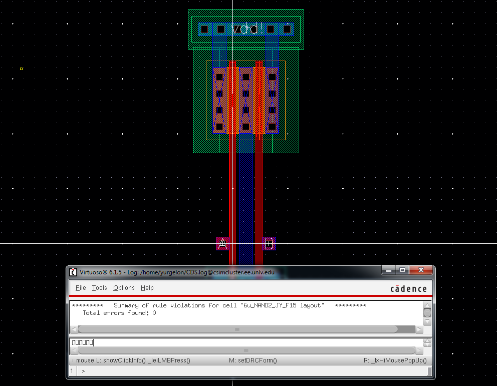
- Below
is the drafted schematic, and layout for the NAND gate. The below
layout is DRC and LVS clean. Refer to the bottom of the section for the
simulation of the logic. This layout xid not take alot of time as the
design only requires a few connections. I did not have any issues
getting it to pass rule checking or LVS.
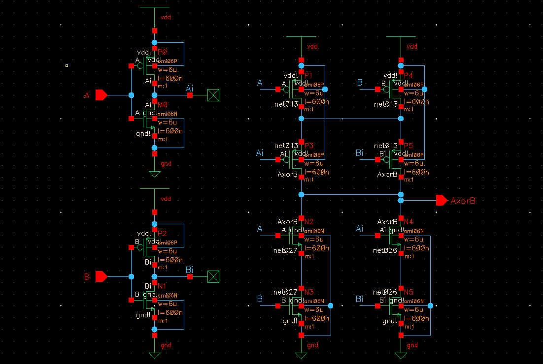
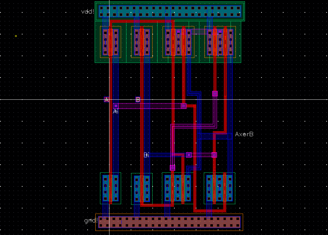
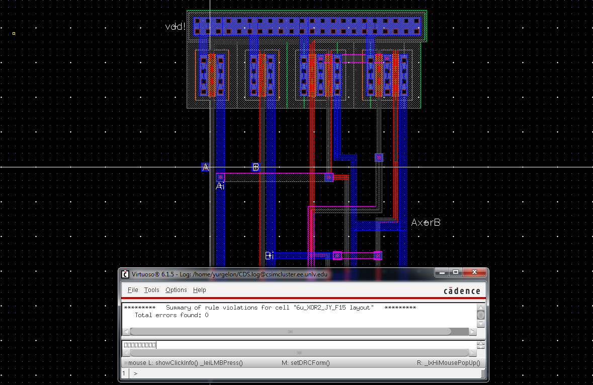
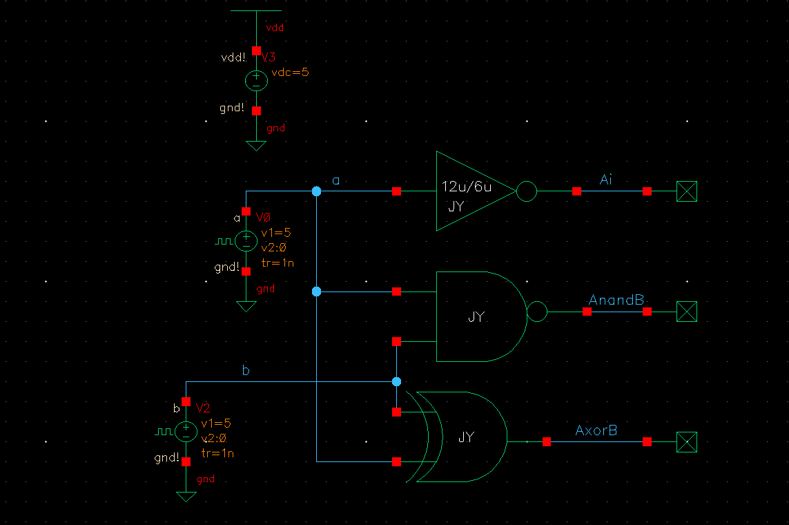
- Below
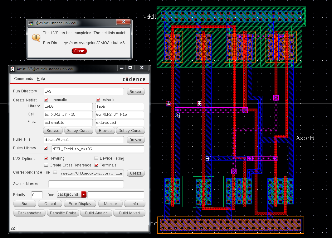
is the drafted schematic, and layout for the XOR gate. The below
layout is DRC and LVS clean. Refer to the bottom of the section for the
simulation of the logic. Laying out this gate was much more difficult
than the NAND gate. I ran into issues with spacing, but after
increasing my cell frame I was able to resolve them. The metals layers
need to be spread out so that they do not violate a rule.
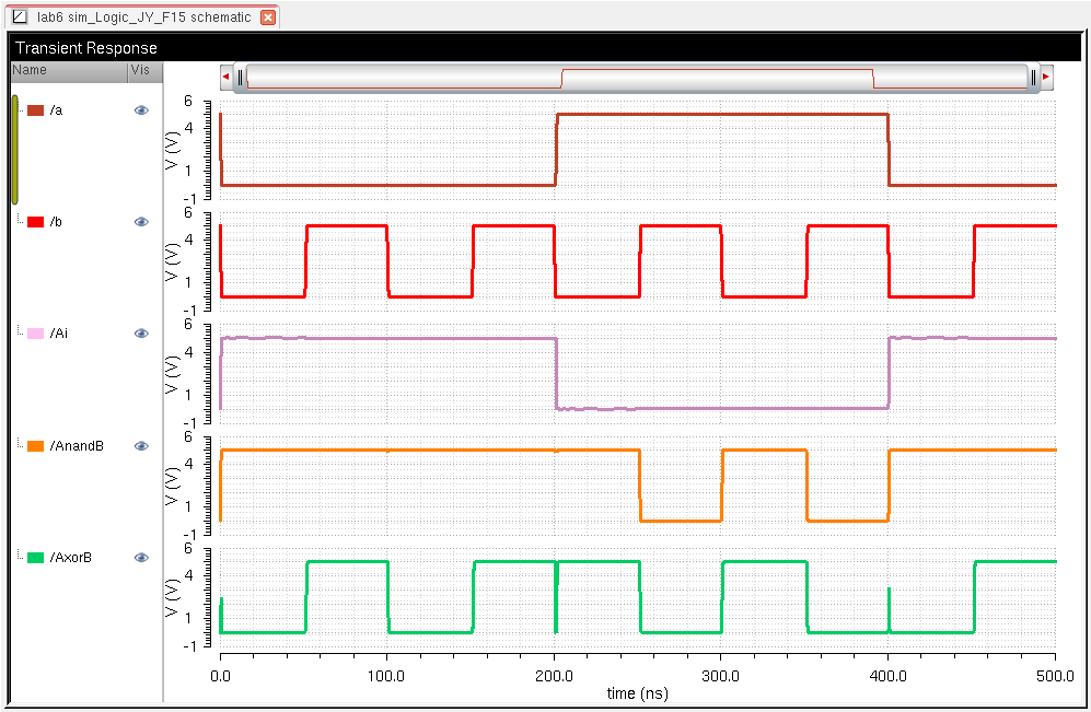
- Below
one can see the operation of all of the logic gates. The glitches
associated with the simulation are a product of the rise and fall times
of the logic gates with their associated inputs.
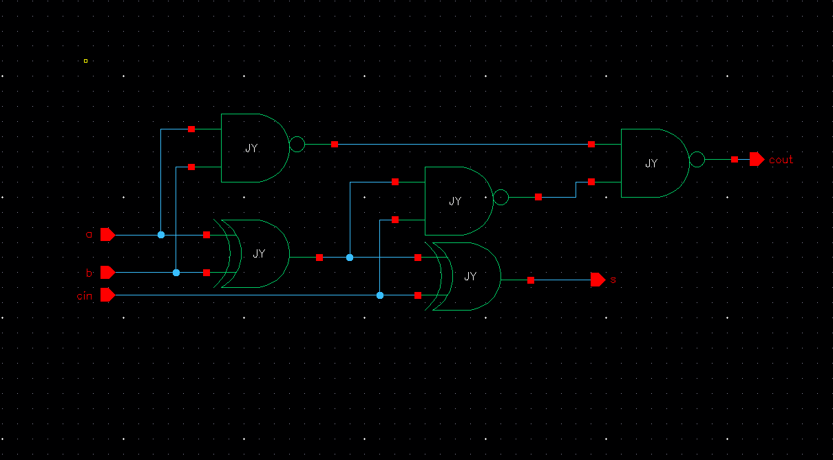
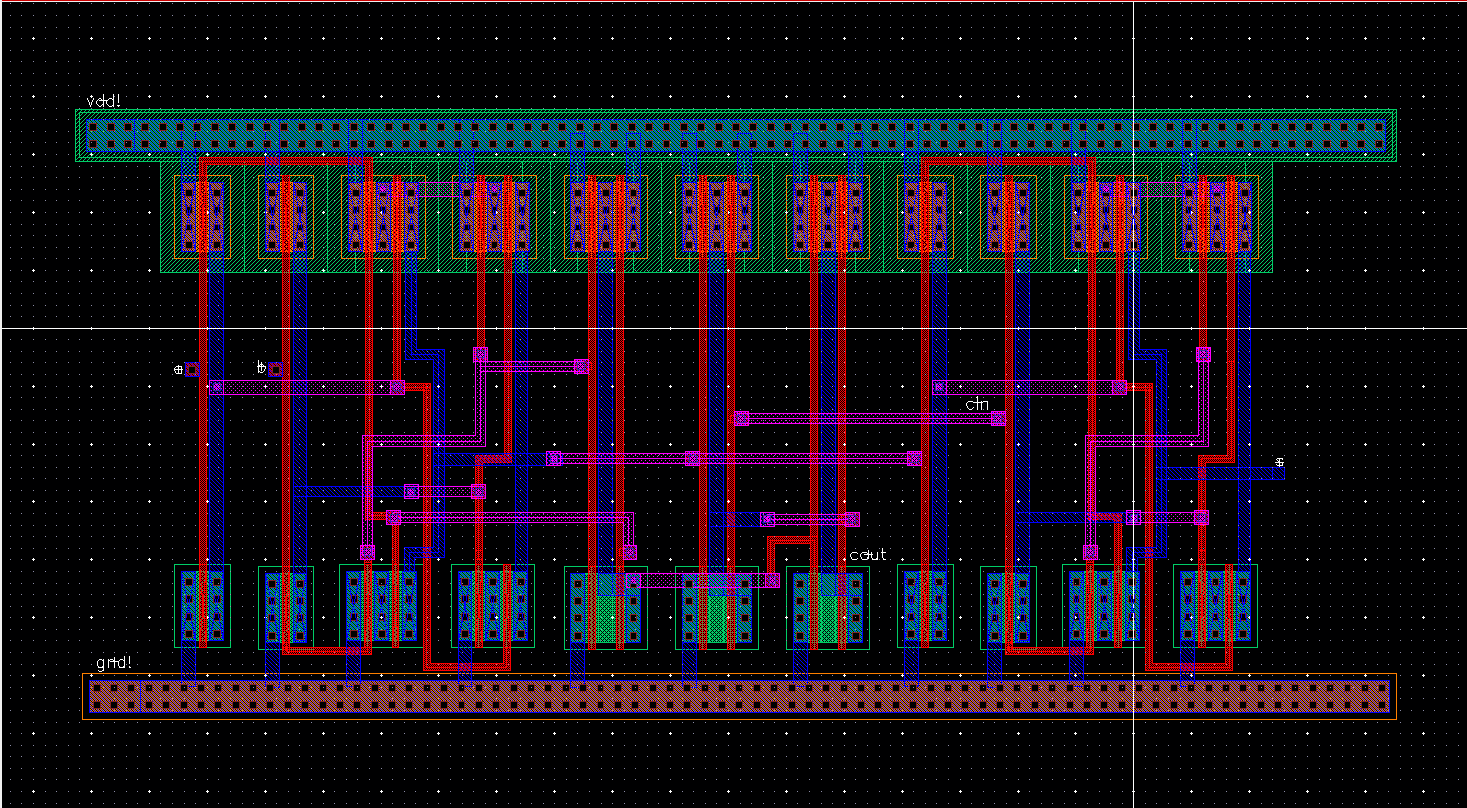
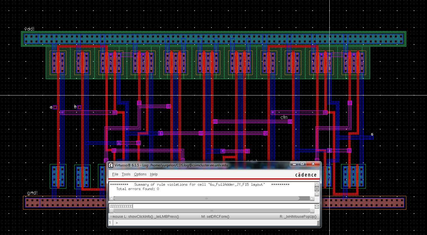
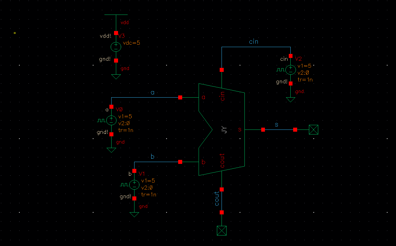
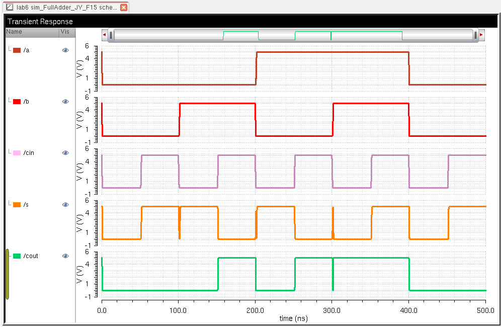
Exercise #2: Using these gates, draft the schematic of the full adder.
- Below
is the drafted schematic, and layout for the Full Adder. The below
layout is DRC and LVS clean. After laying out the XOR and NAND gates
individually, the Full Adder did not cause any issues. I simply had to
lay them out in accordance to the standard cell fram, and then connect
the remaining connections. Refer to the bottom of the section for the
simulation of the logic. The simulation below functions through all the
various states of the Full Adder and holds true to the truth table. The
slight glitches on the simulation are due to rise/fall times of the
internal gates. In this case, by stringing together multiple gates, we
start to have propagation delays in the overall device.
Return to EE 421L Labs