Lab 5: Design, Layout, and Simulation of a CMOS Inverter - EE 421L
Authored By: Joey Yurgelon
Email: yurgelon@unlv.nevada.edu
September 27th, 2015
Pre-lab Work:
- Back-up all of your work from the lab and the course.
- Go through Tutorial 3 seen here.
Lab Description:
- Students
will simulate and layout CMOS inverters of various sizes in the C5 process.
Lab Requirements:
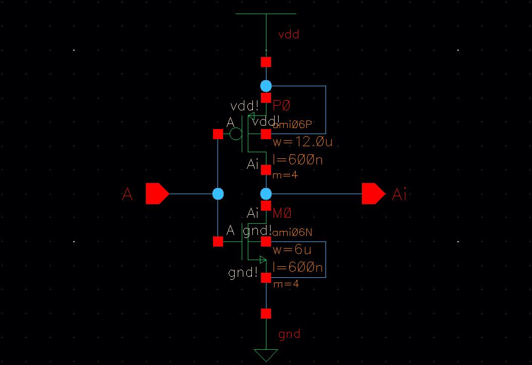
- Draft schematics, layouts, and symbols for two inverters having sizes of:
- 12u/6u (= width of the PMOS / width of the NMOS with both devices having minimum lengths of 0.6u)
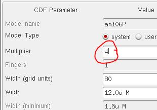
- 48u/24u where the devices use a multiplier, M = 4 (set along with the width and length of the MOSFET, image), as seen below
- Your schematics should have two pins, e.g., A and Ai
- Your layouts should have 4 pins: A, Ai, vdd!, and gnd! (note how lowercase letters are used for power and ground)
- Your
lab reports should document your efforts and results including showing
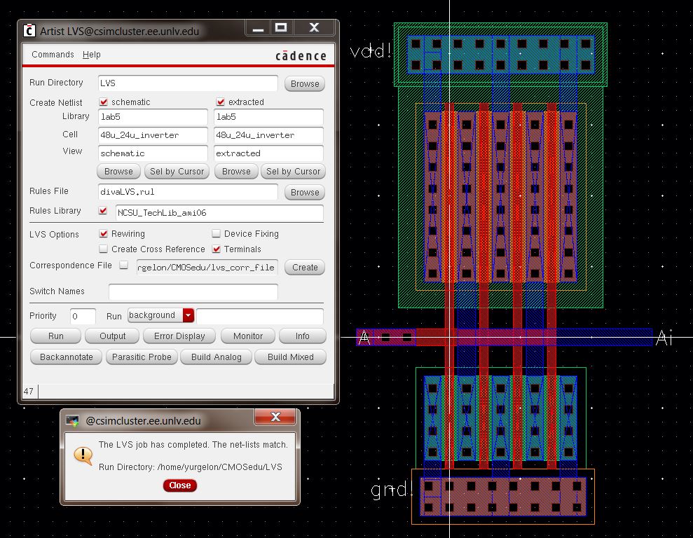
that the extracted layouts and schematics LVS correctly
- Zip up these cells in a directory call lab5_rjb.zip (last two or three letters are your initials) and link to your lab report
- Using SPICE simulate the operation of both of your inverters showing each driving a 100 fF, 1 pF, 10 pF, and 100 pF capacitive load
- Comment, in your report, on the results
- Use UltraSim (Cadence's fast SPICE simulator for larger circuits at the cost of accuracy) and repeat the above simulations
- Use Setup -> Simulator/Directory/Host and select UltraSim as seen below
- You'll also have to point to the MOSFET models again as seen below
- Note that UltraSim only performs transient simulations (not AC, Noise, DC, operating point, etc.)
- Not knowing this last item will lead to wasted time if trying to use UltraSim exclusively for simulations
- ALL OF THE DESIGN FILES ASSOCIATED WITH THIS LAB CAN BE FOUND HERE.
Experimental Results:
Exercise #1:
Draft schematics, layouts, and symbols for an inverter of the size:
12u/6u (= width of the PMOS / width of the NMOS with both devices
having minimum lengths of 0.6u)
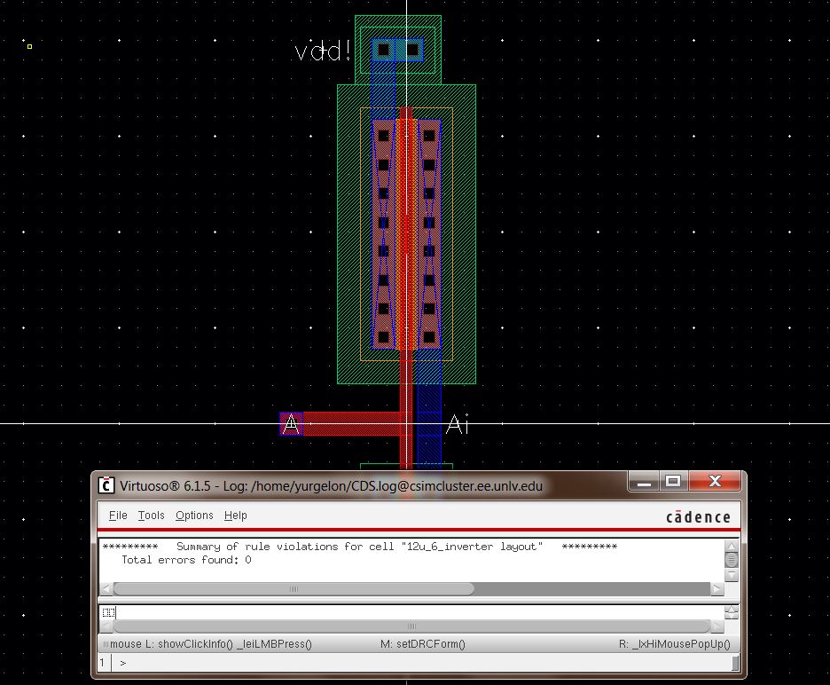
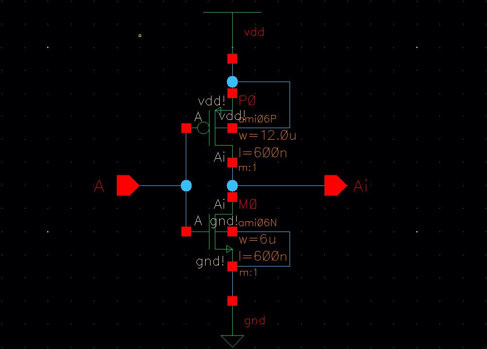
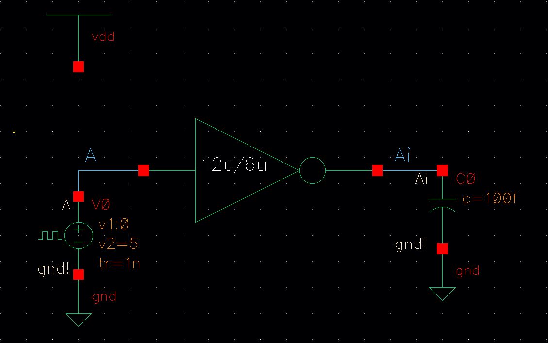
- Below
is the drafted schematic, and the test schematic used in the following
simulations. In this case a 100 fF capacitor is added at the output,
but the simulations take note of all of the other loads as well. The
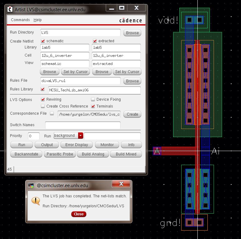
layout was both DRC and LVS clean.
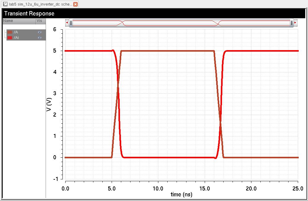
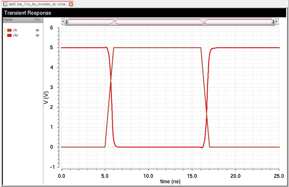
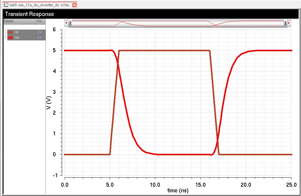
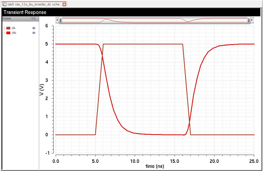
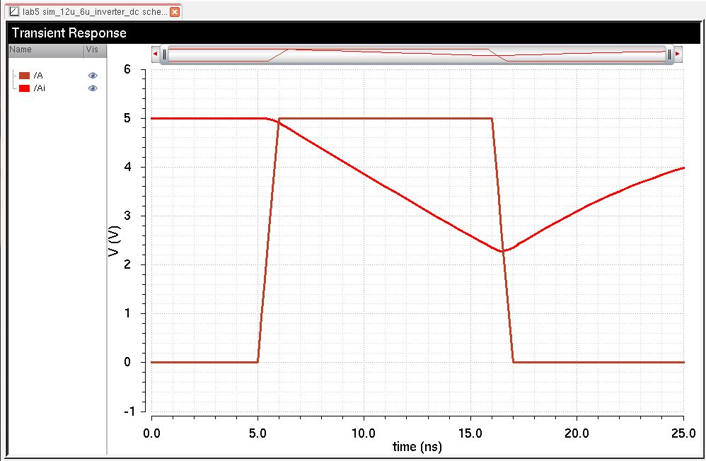
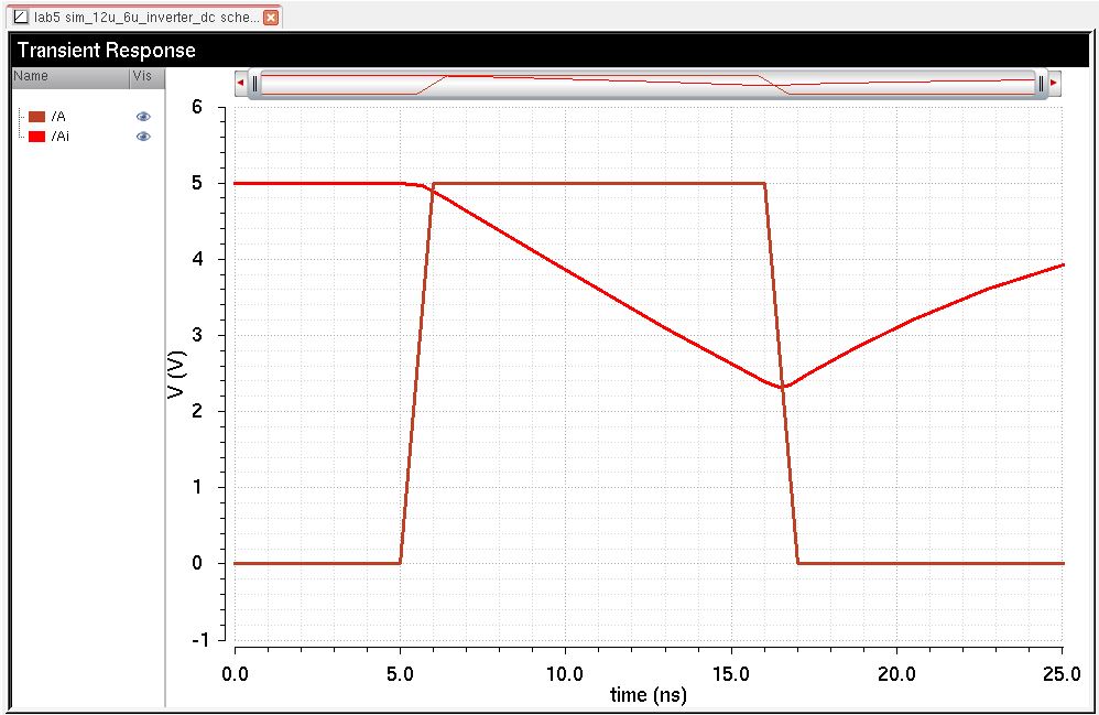
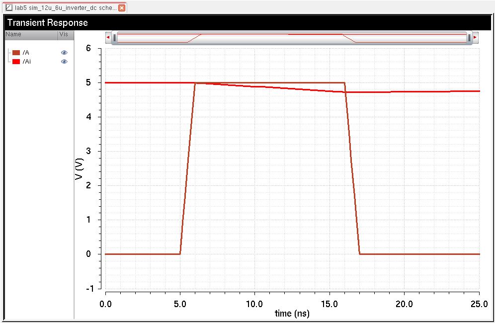
- Below
are the simulations that characterize the performance of the inverter.
On the left side, the simulator used was Spectre, and UltraSim on the
right-hand side. The simulations show how the response of the inverter
changes with an increasing capacitive load on the output. Each row of
simulations increases in the load simulated. The load is as follows:
Row #1 - 100fF, Row #2 - 1 pF, Row #3 - 10 pF, and Row #4 - 100 pF. It
can be easily seen that with an larger capacitor value, the inverter
has a hard time fully driving the load. By the time we get to a 100 pF
load, the inverter cannot fill the bucket fast enough.
One will notice that the inverter cannot source the amount of current
to properly drive the load. This can be fixed by increasing the widths
of the MOSFETs, however. One can see this in the larger inverter below.
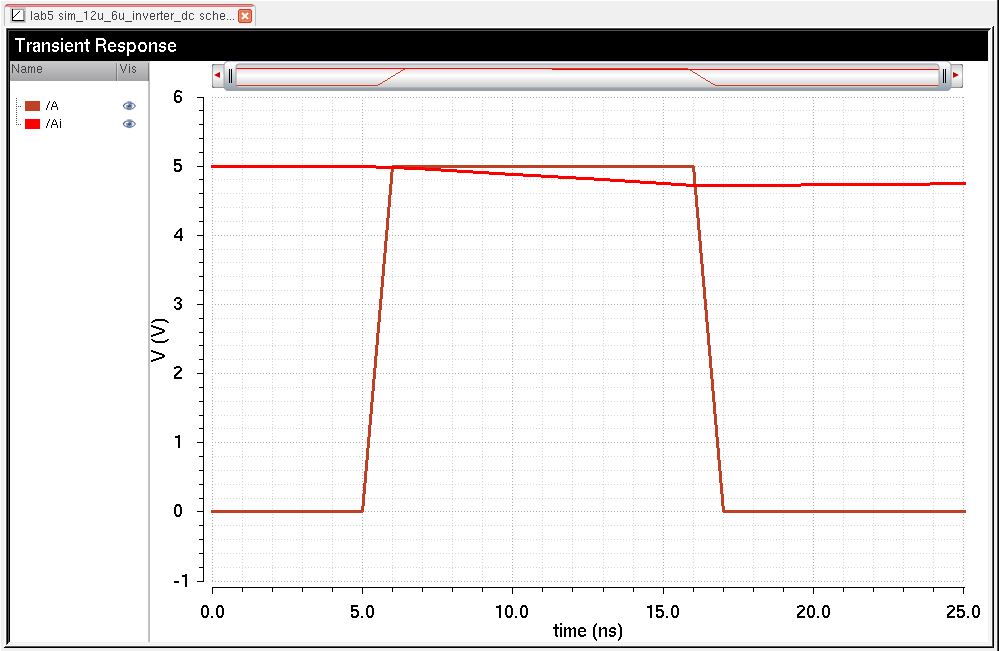
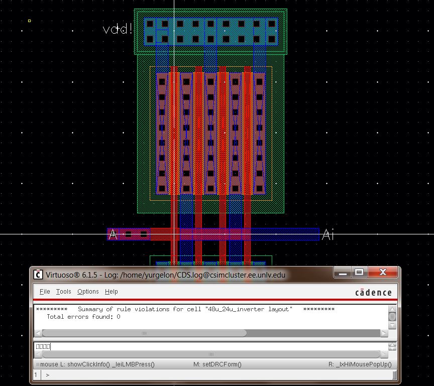
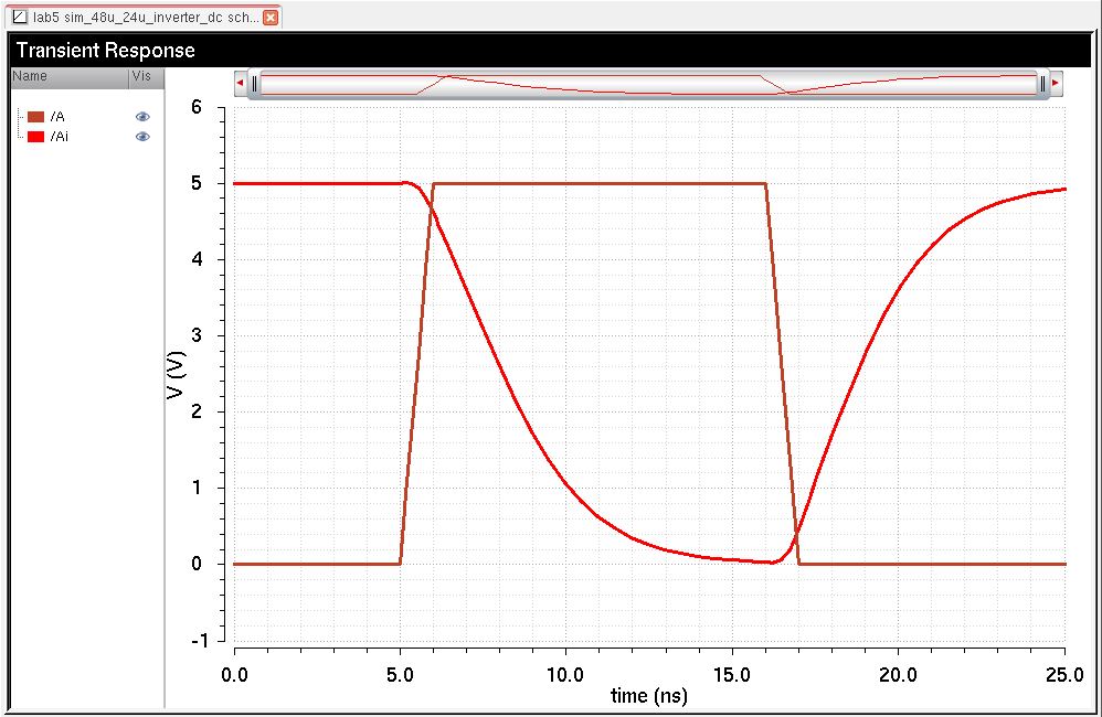
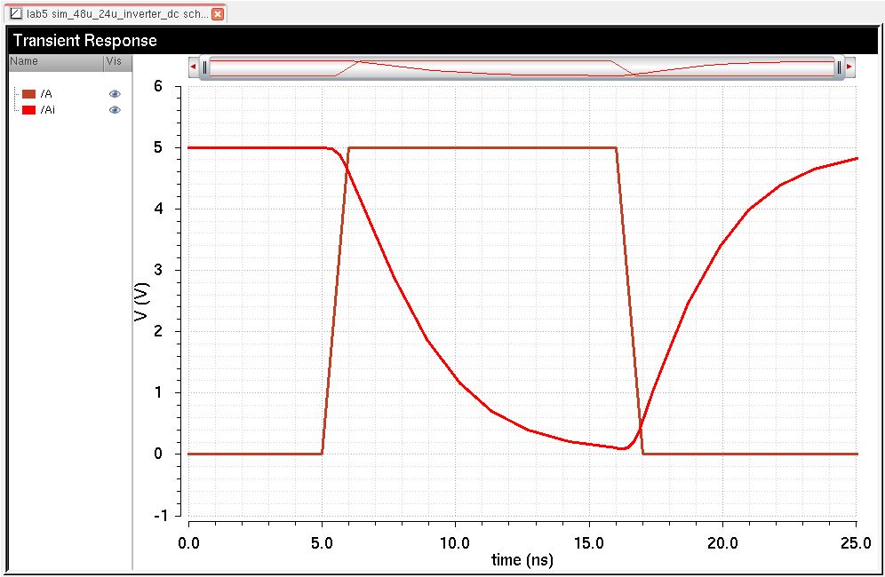
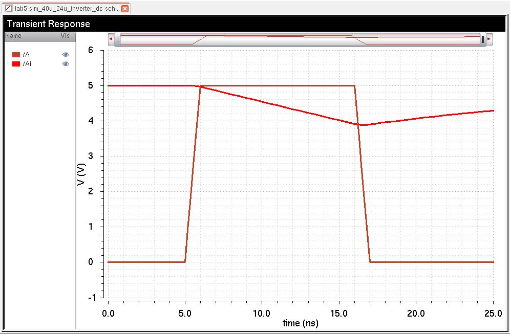
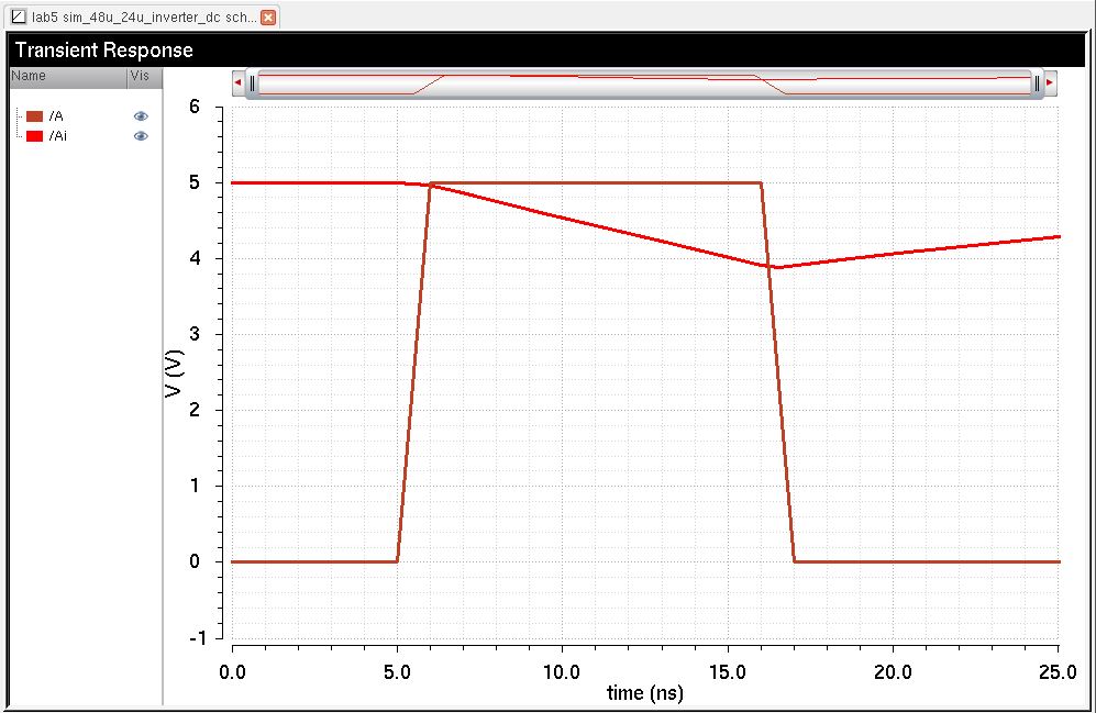
Exercise #2: Draft
schematics, layouts, and symbols for an inverter of the size: 48u/24u
(= width of the PMOS / width of the NMOS with both devices
having minimum lengths of 0.6u)
- Below
is the drafted schematic, and the test schematic used in the following
simulations. In this case a 100 fF capacitor is added at the output,
but the simulations take note of all of the other loads as well. The
layout was both DRC and LVS clean.
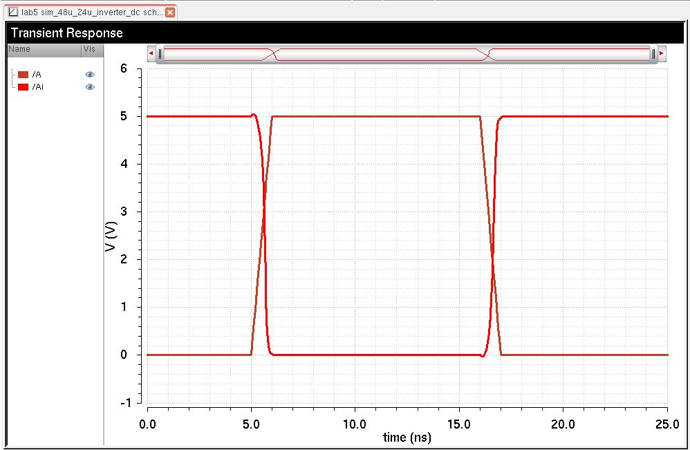
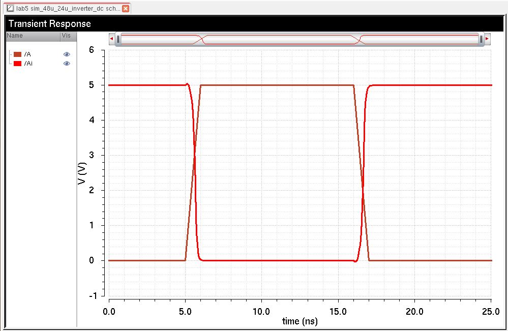
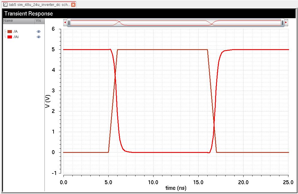
- Below
are the simulations that characterize the performance of the inverter.
On the left side, the simulator used was Spectre, and UltraSim on the
right-hand side. The
simulations show how the response of the inverter changes with an
increasing capacitive load on the output. Each row of simulations
increases in the load simulated. The load is as follows: Row #1 -
100fF, Row #2 - 1 pF, Row #3 - 10 pF, and Row #4 - 100 pF. Due to the
increased widths of this inverter, with the M multiplyer (Adding FETs
in parallel), the device is able to source more current than the 12u/6u
inverter. This results in better simulations with the increasing loads.
Even though we increased the width, however, we still cannot drive 100
pF correctly. With the speed of the pulse tested, we would need to have
an off-chip capacitor or increase the multiplied of the inverter
further.
Return to EE 421L Labs