Lab 3: Layout of a 10-bit digital-to-analog converter (DAC) - EE 421L
Authored By: Joey Yurgelon
Email: yurgelon@unlv.nevada.edu
September 14, 2015
Pre-lab Work:
- Back-up all of your previous work from the lab and the course.
- Finish Tutorial 1 seen here.
Lab Description:
- Students
will learn how layout the DAC produced in the previous lab.
Lab Requirements:
- Use the n-well to layout a 10k resistor as discussed in Tutorial 1
- Discuss,
in your lab report, how to select the width and length of the resistor
by referencing the process information from MOSIS
- Use this n-well resistor in the layout of your DAC
- Discuss, in your lab report, how the width and length of the resistor are measured
- Ensure
that each resistor in the DAC is laid out in parallel having the same
x-position but varying y-positions (the resistors are stacked)
- All input and output Pins should be on metal 1
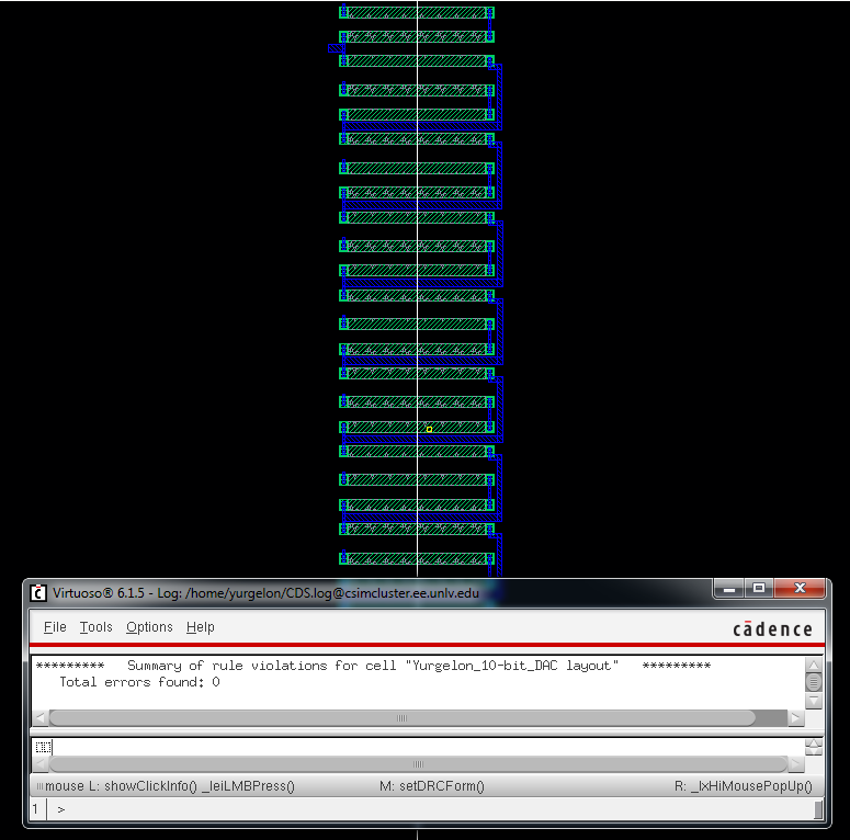
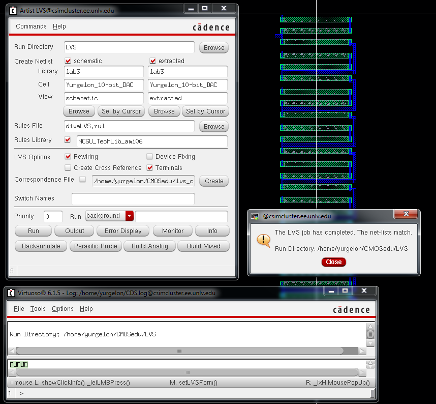
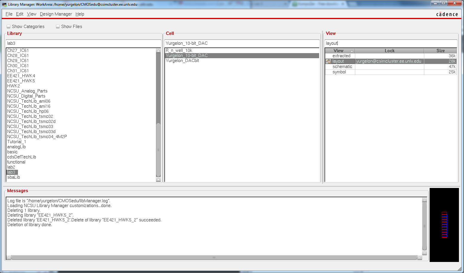
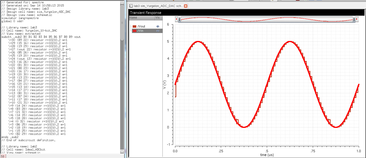
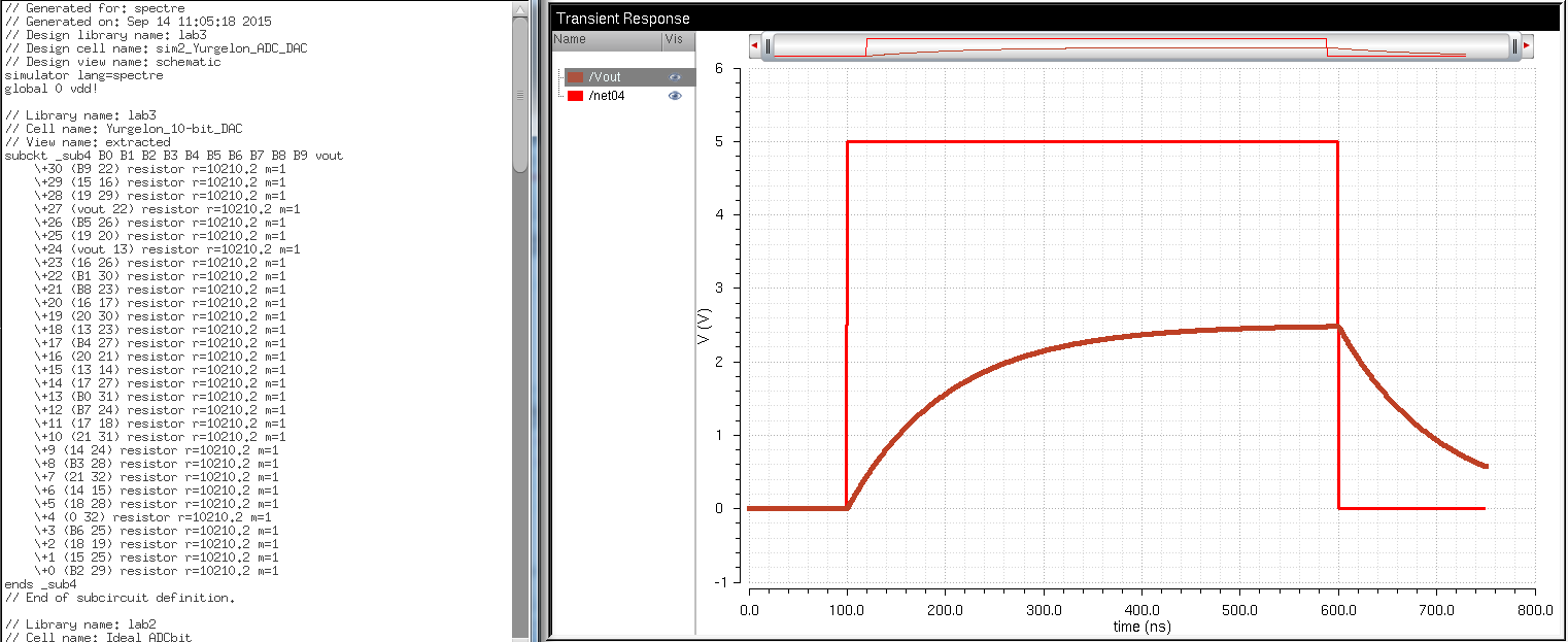
- DRC and LVS, with the extracted layout, your design (show the results in your lab report)
- Zip up your final design directory and place it in
the lab3 directory, with a link on your lab report, so the grader can
examine both the layout and schematic (and simulations)
THE ZIPPED FILE CONTAINING ALL OF THE PROJECT FILES CAN BE FOUND HERE.
Experimental Results:
Exercise #1:
Discuss, in your lab report, how to select the width and length of the
resistor by referencing the process information from MOSIS.
- To select the width and length of the device, we need to use the corresponding equation: R = (p/t)*(L/W).
The (p/t) term corresponds to the sheet resistance of the process in
use which happens to be 800 Ohms/square. From the equation, we can then
see that the selection of the length and width will now relate to the
total resistance of the device. Since MOSIS requires a factor of 12*300
nm or3.6 um for the minimum width , we used this as a fixed value for
our equation. After rearranging the equation, the length needed to
produce the desired resistance can be calculated. Refer below for the
dimensions used.
- To measure the device, one can use the
shortcut 'k' to pull up a ruler. By clicking on a starting and ending
point, one can then find the distance. This was used below to verify
the calculations done in the previous step.
 |
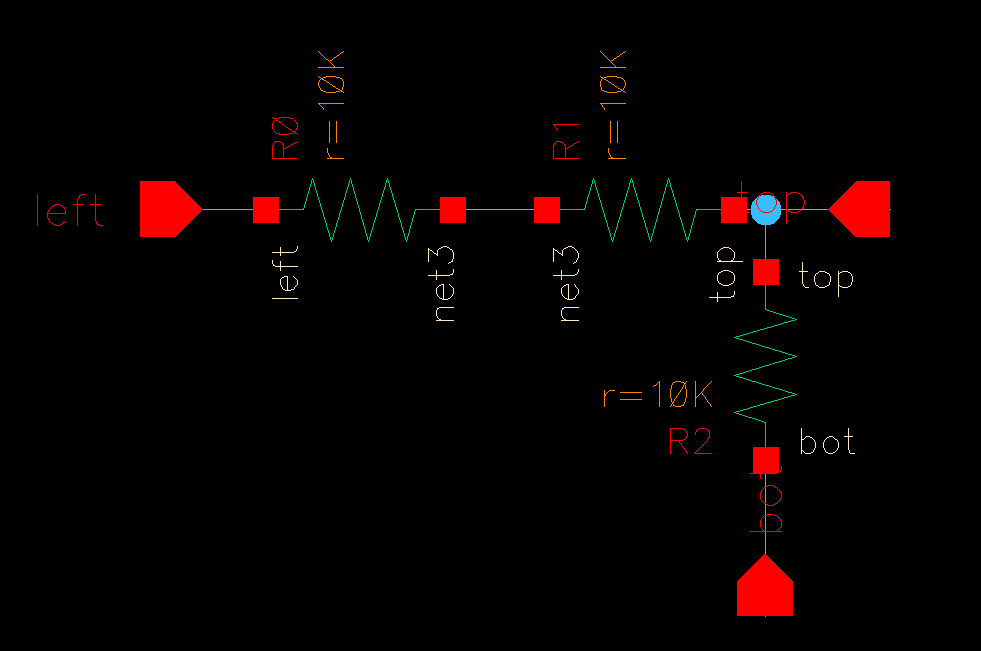
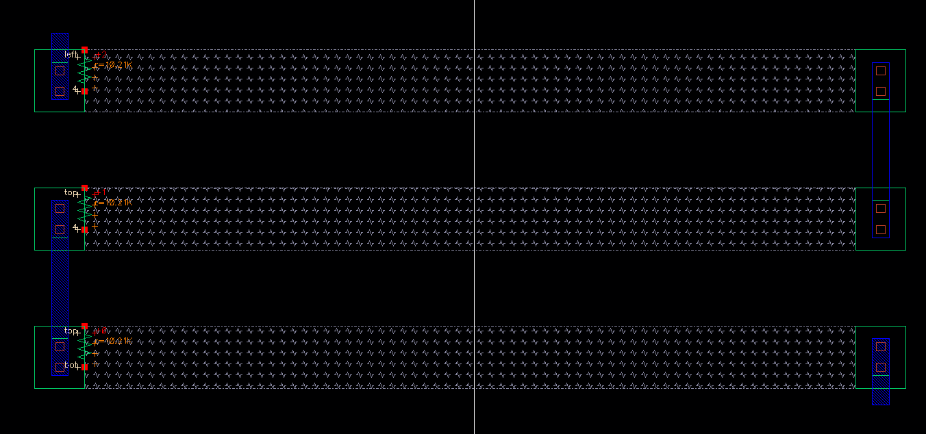
Exercise #2:
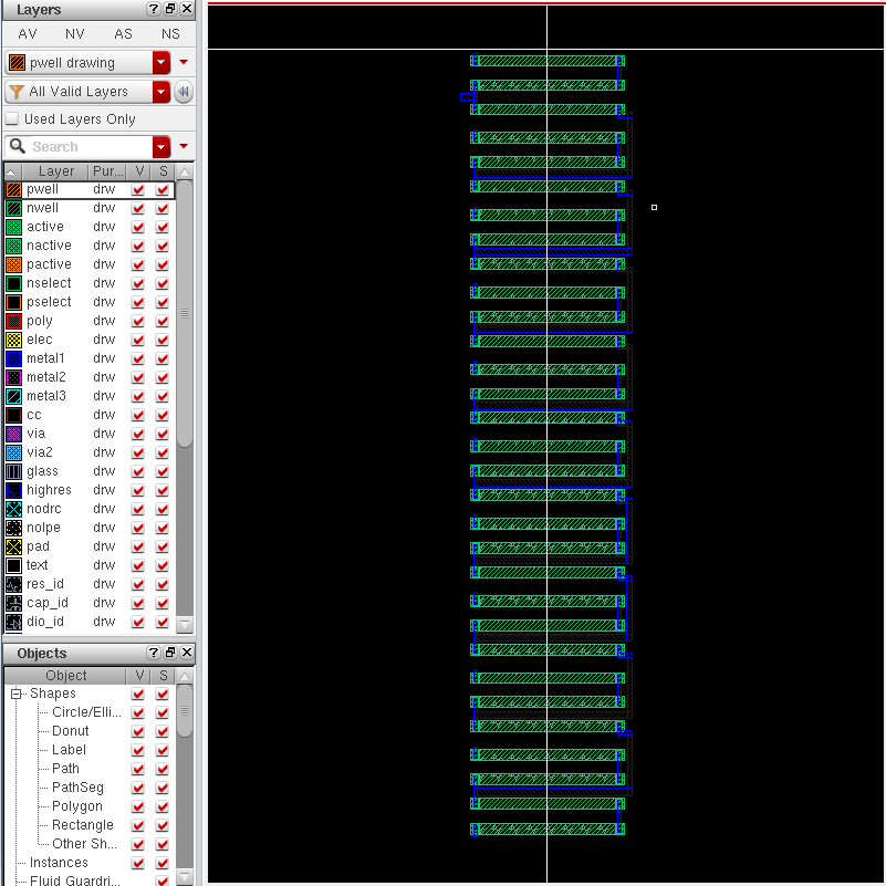
Ensure that each resistor in the DAC is laid out in parallel having the
same x-position but varying y-positions (the resistors of stacked). All
pins should be on metal. DRC and LVS, with
the extracted layout.
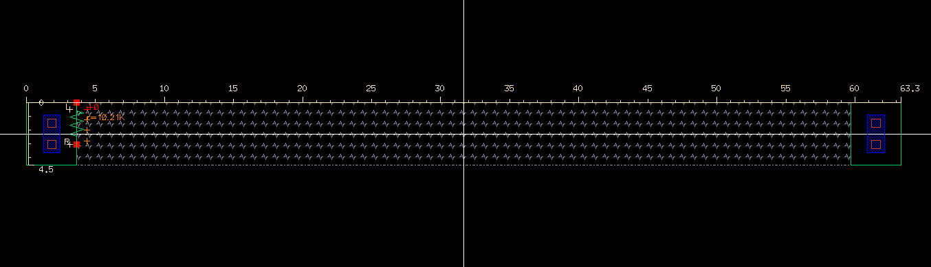
- The
layout for the DAC was very straightforward. I first started with the
layout of a single DAC_bit. From there, I could instantiate the DAC_bit
layout into a 10 bit_DAC layout in an array. This produced all of the
necessary bits for my device. From here, I just needed to connect the
metal to the appropriate positions, and label all pins.
Return to EE 421L Labs